New PCBs

The PCBs arrived this week.  I really like the way my Logo came out.  20160415BarePCB
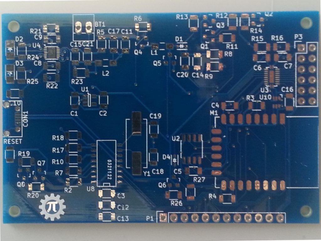
I do want to make an adjustment, make the arrows larger, they didn’t even show up on the silkscreen.

PCBLogo

To start testing, I put a jumper in bypassing the lithium cell charger. I then installed the ESP-12E, the SPI RAM, The Crystal, the USB Serial Bridge, the voltage regulator, and the USB connector. Just enough to power up, load a program and test the basics.

20160415assembledPCB

First test was to  connect to PC and run ESPlorer– it worked.

I got a message:


AT-based firmware detected.
AT+GMR
AT version:0.40.0.0(Aug 8 2015 14:45:58)
SDK version:1.3.0
Ai-Thinker Technology Co.,Ltd.
Build:1.3.0.2 Sep 11 2015 11:48:04

I then tried to install my test version of the software and it wouldn’t install.  I went back to ESPlorer and started playing with the DTR and RTS to see what would happen. It turns out I got DTR and RTS backwards. So I cut the traces and added a couple of jumpers. This is the kind of mistake I was hoping to catch in the design review.

It programmed great with the wires swapped. My code crashed, back to a “Hello World” version.

Turns out the internal memory chip installed on the ESP-12E does not run at the settings I had specified with esptool.py.  I found this out by setting it to 20MHz DIO mode which started working. I then switched it to QIO mode to see what happened. QIO worked, next I tried running at 40 MHz. That worked.

../esptool/esptool.py --port /dev/ttyUSB0 --baud 230400 write_flash -ff 40m -fm qio -fs 32m 0x00000 ../bin/eagle.flash.bin 0x40000 ../bin/eagle.irom0text.bin

I enabled HSPI Overlap mode by adding spiRamInit() to the end user_init(). Ran without crashing. When I started building for use, I discovered no SPI Master Read available.  I saw something that looked correct for slave read, so I borrowed a line from it and did a write followed by that line– it built. I uploaded the code, and it ran, still no testing of the SPI Ram.

I added the function calls to write “Hello World” to the SPI RAM. and read back and put out to the console. and I got garbage back to the console.  Not a surprise. Debugging with a logic analyzer next week.

Have you written code for the ESP8266. Have you worked with SPI before? I would love to Hear from you.


Design testing for layout

I tested the battery charging circuit this week. It failed.  The lithium cell would charge, but when I disconnected the power adaptor everything shut down.  I didn’t understand how the enable lines worked.  In my hurry, I missed an example circuit in the datasheet that closely matched my needs. Most importantly it showed where to connect the enable lines for “normal” operation.

So for my client, I connected a diode from the out line of the chip to the in line of the chip(where the enables were connected to). The diode makes sure the out line is controlled by the chip and it can manage the current correctly.  Note D5 in the schematic below.

D5addition

This works but it is kind of a hack.  Hacks are great for testing prototypes, doing one off designs, and temporary changes.  Hacks lead to problems in production, if at all possible hacks should be avoided on production runs.  The right way to connect this circuit for both the programmer and my client is to connect EN and ENO to the +5V rail and ENBAT to the battery positive terminal.  This configuration means that anytime power is connected to the power, it will supply system voltage from the +5V supply and charge the lithium cell with whatever current is left from the 450 ma I limited it to.  When the +5V rail is not powered, or under powered,the lithium cell supplies current to system.

LithiumChargerFixed

I modified the code to connect the sigma delta to GPIO13 to drive the level shifter signal, then connected 5 Volts to the Vt and measured the waveform on the pad that corresponds with GPIO 13 through the level shifter. It didn’t work, Or the DSO138 oscilloscope can’t read the sigma delta signals.  I found a recommended power up sequence of the the level translator chip that I hadn’t considered before, the /OE pin should be brought low after power up.  This is to prevent excessive currents, I shouldn’t get the results I am seeing, I decided to try just toggling the GPIO12, 13, 14 pins controlled by the serial communications.  The system has gotten very unstable, I decided to re-flash the user config and wifi calibration data.  Turned out that Vt was/is shorted to ground, My best guess is the Pad directly under the chip solder bridged to the Vt(Vccb) pin of the level shifter chip.  Time to lay out again.

Do you have any Ideas or suggestions that might be useful for this design? Would you do anything differently?

Debugging

I got the Sigma Delta putting out a waveform that I was looking for. But when I connected the power rail to the input of the inductor for voltage boost, the system stopped booting correctly.

I had several possible problems to look at.

GPIO16 is tied to reset on some ESP8266 modules allowing wake from deep sleep based on the RTC. I tried taking it back out of the code and I am still getting unexpected boot up activity. Doesn’t appear to be the problem, I may have to come back and have another look.

I haven’t built with the change of memory maps until last week. The bootloader may not be linking properly with my code or I may have made some mistakes pertinent to the linker. I removed the new files and recompiled without GPIO16 support and therefore a smaller memory map that fits without modification of the link files. I commented out most of the code and it still would not boot into my code. Code doesn’t appear to be the problem.

Finally, the boost circuit may draw very large amounts of current that will cause noise back into the rest of the system.  Power may not be stable enough for reliable operation. I disconnected the 5V from the boost circuit and got reliable boot.  I need the boost circuit to work, so I replaced the 10 ohm resistor with a 68 ohm resistor( Maximum current draw from USB would be 5v/68Ohms or 74mA). It wasn’t enough. So I tried 220 Ohms, then I tried 1KOhms.  This means the maximum current I can provide to VPP is significantly reduced.  I will add capacitance to the PCB on the 5V lines to allow for better noise immunity. The board is booting reliably.  The problems I had earlier with the CH340G were probably related to this problem as well.  I still needed to run the CH340G at 3.3V, So I am glad I changed that already.

The boost circuit is not able to create a voltage above 5v with the 1K resistor. Testing the ADC reading, I discovered I had R8 and R9 Cross labelled on the board. So I switched the labels on the layout.

The firmware is running again.  I can put a pulse stream out to the Voltage Boost circuit but the 1K limiting resistor is too large to work correctly.


MIT License applied to hardware

The MIT license gives a lot of freedom to developers to use the intellectual property in any way they want.  This includes manufacturing, selling, and modifying the design. It does not require or restrict attribution. It does give the designer some protection for liability.  This is not compatible with more restrictive licenses.


The reasons I want to design this product include:

  • Teaching about electronics design
  • Create a low cost universal In Circuit Chip programmer

If some company picks up this design and produces it at a fair price then both objectives are met. This would create a well documented hackable device for a very reasonable price.

The MIT license for software and hardware is compatible with my goals.

If I want to integrate some other design with more a restrictive license, I would have to switch to the more restrictive license or separate the other design into a module or in the case of software a library.

I will continue to look at other software and hardware licenses.