Post 100

Statistics

I have been writing this blog for almost two years now.  With only about two hundred views per month. Of the two hundred per month, only about twenty five are returning visitors. I have received six real comments in this time.(and tons of spam comments)

I was hoping to get more comments to help me know what is interesting to the people that do make it to my site.  Also, I am not a writer, I am unsure if I am giving too much information or not enough.  These statistics are a little disappointing, but I will continue to write and hopefully improve my skills.

Status Update

The boards are fabricated and have been shipped from PCBWay.  I am looking forward to testing the changes  I have made to the layout.  While doing some testing, I hooked up the lithium cell backwards and fried the charger chip. I replaced it and the board is back up and running.  I have ordered the new level translator chip so I will be able to test it when the new boards come in.

Looking Forward

As I build it this next time, I will be looking for ways to make it less expensive and more reliable.  One thing I would like to improve is how easy the board is to solder, the lithium cell charger is very difficult to solder.

In the coming weeks, I plan on re-testing the hardware, Improving the software, and doing some functional testing.  In essence, I am hoping to move from prototype stage to alpha stage.  The software should start to look like the final product and the electronics shouldn’t need to change much if at all.

Goals:

Continue reading

Layout check … continued

With the new check plots I made last week, I checked the layout net by net like I did back in Sept 5, 2015. I am still uncertain about the pinout of the ESP-12F modules. To test it, I removed the ESP-12E installed on the board I am currently using, and replaced it with a new ESP-12F.  I had to be careful that the jumper wires all got back to where they were before removing the module.

The new module programmed first try but didn’t boot correctly.  I had forgot to upload default values, the flash comes programmed for a different memory layout.  Once I installed the default settings, it booted up correctly.  I had removed the test for HSPI/SPI RAM, so I went back into the code and re-enabled the Hello World ram test.

I went into serialInit() and changed the line DISPLAY_MENU(); to DISPLAY_MENU_W_SPI(); Re-compiled and tested.  Unfortunately the result was not “Hello World”. When I cleaned up the code, I made the write to SPI RAM easier, but I need to initialize the hspi.  I started connecting my mixed signal oscope to analyze what was happening on the SPI bus.  And… I found a loose jumper wire.  The one that connects the chip select between the ESP-12F and the SPI RAM. Once this was connected, the extra stuff I had put into the software became unnecessary.  I deleted the extra code and it works just fine.  The firmware is back to where it was before I started testing. There are no changes to upload.

This means that the circuit is tested and the current layout is ready to send to fabrication.  I zipped up the gerber files. Then checked pricing with PCBway, DFRobot, and Seeed Studio.  With shipping PCBway came in a little less at US $19.  With PCBway, I have to wait for a design review before they will give me a final price and allow me to pay for it. Usually this is pretty quick but depends on the day it is submitted.

Have you bought boards from Chinese manufacturers? How quickly did you get them?

Layout Verification (Hardware V00J)

The changes I made to the layout last week were pretty extensive especially concerning the level shifter IC. I don’t want to do layout verification, but It needs to be done. Like when i did the check plots before, I printed out the schematic and each layer. Then I physically traced the circuits both on the schematic and the layer plots.  I use colored pens to help differentiate each net.  Before printing, I removed the note from the schematic about testing the lithium cell charger.

I plotted the top copper, bottom copper, top silk, and Edge cuts layers to PDF file and imported them into gimp. I then removed the white background from each layer, and then put a new layer at the bottom layer filled with white. I left the board outline unchanged.  Then I changed the top silkscreen layer to yellow, and faded the copper layers to about 25% black.  This allows me to see the color of the pens while I am tracing the circuits.

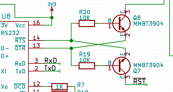
I found that I hadn’t updated the RTS and DTR lines used in programming. They were swapped and I changed them on the board when I received the new PCBs on the last spin.  So I had to go back into the schematic and change them.  I vertically swapped the cross linked transistors and resistors R19,20, Q7,8 on the schematic so that effectively RTS and DTR are swapped. I re-ran the netlist, imported it into PCBNew and proceeded to make the adjustments to the layout.

rtsdtrswap

As I was looking at the layout, I was able to see a cleaner layout of these parts. So I made the adjustments.  Also, I remembered I wanted to modify my logo on the board.  The arrows aren’t visible on the silkscreen, so I went back into Gimp and edited them to make the gap bigger.

dtrrtsswappluslogo

Unfortunately PCBnew renders the pad on top of the silkscreen so you can’t see the new arrows.  I re-printed the schematic and layouts just like I did this week and I will check the layout again before I order another spin.  I am glad I caught this mistake now and not after the next spin of the board.  As before, the intellectual property for the Uprogrammer is still licensed with the MIT license. My logo is my trademark and I reserve all rights.

Because the schematic and layout have both changed, I have uploaded a new version to Github.

Do you like to “clean up” your layouts when checking them?  Are you doing any layouts at this time?

Update layout Hardware V00I

Finally time to update the layout.  The charging circuit works well and I changed the level shifter on the schematic last week. So this week, I updated the layout.

I started by generating a new netlist. Next, I ran CvPCB to verify all the parts had footprints associated with them. They all do. Next I ran PCBnew and imported the netlist; making sure the exchange footprint settins was set to change.  I got an error:

Error: Component 'U3' pad '~' not found in footprint 'Housings_SSOP:TSSOP-20_4.4x6.5mm_Pitch0.65mm'

I had to figure out what that means before moving on.  It suggest one of the pins was named wrong either in the schematic symbol or the footprint library. I checked the schematic symbol first. I noticed the GND pin didn’t have a pin number assigned to it. Easy fix, added it and updated the library. I set the GND pin number to 11, saved it to the library, made sure it was in the schematic correctly, and re-generated the netlist.  I had to delete it and re-place it into the schematic to correct the schematic.  This meant that CvPCB no longer knew the footprint to use, so I updated it and re-generated the netlist again. No more errors in PCBnew import of the netlist.

I started by ripping up the unconnected traces. Then I started placing footprints.  I hid the bottom layer to make it easier to see what I was working around on the top layer.  Once I had the parts placed, I started routing traces.  I had to adjust component placement a few times to get everything to fit.  As I got to a point that I couldn’t do all the traces on the top side of the board, I un-hid the bottom layer.  While I was working with both sides, I had to re-fill the zones several times to correct for the areas I added new traces on the bottom side.

I finally got to 0 unconnected nets. I did a quick look to make sure all the references were readable and not under other parts.

layoutv00i

I plotted out the Gerber files and did a quick check to see if it looked OK and got ready to order.  When I look at Gerbers, I am looking for broken traces and unintentionally connected traces.  I used Gerbview to do this check. As I went into Gerbview and tried to load the files, the were double of all the files.  It looks like the developers of KiCad decided to change the naming conventions  for output to gerber.  I went in and deleted all the files in that folder and re-ran the plots.  While looking at the gerber files, C10 and U3 references were covered up.  I went in and fixed them and re-plotted.  While I was at it, I discovered U10 wasn’t anywhere near it’s footprint.

I created a zip file with the plot files ready to upload to a fabrication house. I have uploaded the files to the github repository, click the hardware link in the right column to go get it.

Are you using Kicad?  What tools are you using to design in?  Do you have trouble finding datasheets for Chinese parts?

Lithium Charger Testing (Hardware V00I)

I installed the Lithium cell charger chip and it’s associated components.  While I was soldering the components, I noticed that R5 wasn’t soldered correctly.  This is the current limiting resistor for the voltage boost circuit.  So I need to retest the boost circuit.

I then attached the cell and the radio led blinked once.(with no connection, this was expected)  I connected the USB from my computer into the circuit and D2 (Red) lit up. This is STAT1 signal from the charger IC. From Table 5 in the AAT3672 datasheet STAT1 on by itself indicates the system is fast charging the lithium cell.  I disconnected the Cell with the USB still connected, both D3 and D2 blinked until I reconnected the lithium cell and the system then went back to fast charge.

I grabbed my DMM and checked some voltages:

From USB: 4.65V (A Little low, but I have connected the Uprogrammer to a long USB cable for convenience)
Output to Board: 4.65 V (Matches input voltage)
Lithium Cell: 3.96 V (Good range for Fast Charge)

These voltages make sense, I am very happy with these results.  I waited a while to check the results again.  While I was waiting, I started doing some testing of the Voltage Boost Circuit.  With Just the boost circuit turned on, I measured 4.64 Volts on Vpp.  I checked the Duty and prescaler and they were set to 0 and 4 respectively.

I then set the duty cycle  and measured the voltage at Vpp

20% : 19.6 Volts
30% : 20.8 Volts
40%: 21.8 Volts
50%: 22.6 Volts

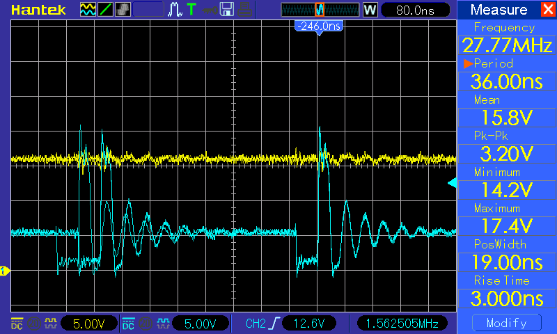
I played with the prescaler and the highest voltage I got was 24 Volts at 50% duty cycle and prescaler set to 9.  This is beyond design specification and has the potential to cause damage to the circuit, I don’t expect to do this in the future. I am happy to know that I have some margin in the design to if I need 20 Volts. I took the following image from my oscilloscope with a Prescaler of 4 and a duty cycle of 10% (25).
pre4duty25

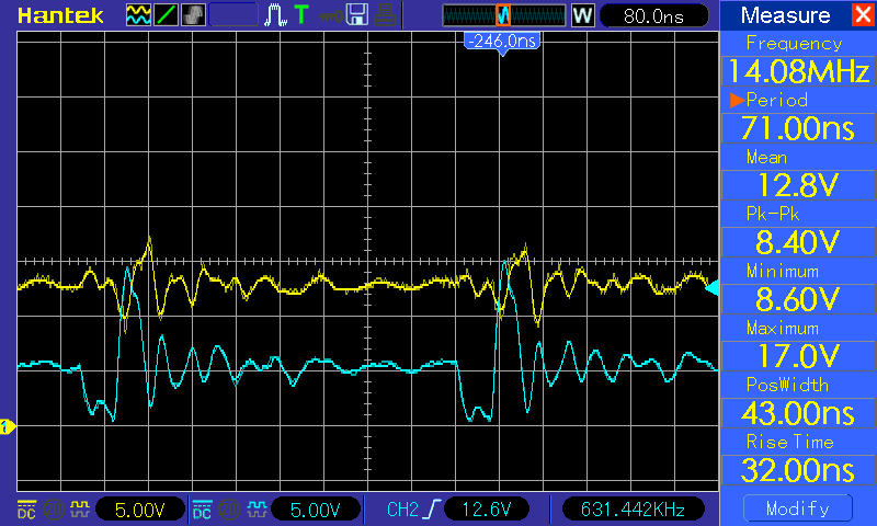
I am not happy with the large steps setting the output voltage of the boost circuit.  I decided to load the circuit with a 10 K Resistor to see how it affected the output voltage.  I soldered a 1206 10K Resistor on top of C20. This lowered the output voltage for 10% with a prescaler of 4 down to 12.8 Volts  But the best voltage I could get out of the system was 18 Volts.  This also made Vpp a lot noisier(See scope image below), I want to add some more filtering.
pre4duty25w10k

I added a resistor to the schematic parallel to C20 and also a place for another capacitor.  The resistor I set the value to 20K as a starting point and the capacitor I set to 1 uF.  The 20 K resistor will draw less current and that should reduce the noise.  The capacitor will also reduce the noise and provide a larger reservoir for current changes when programming a target device.

After doing all this testing the lithium cell voltage was at 4.12 V. This is near a complete charge, I expected the system to go to complete charge very soon. This is indicated by the Green LED being on alone.

After it switched to charge complete, I grabbed my DMM and checked some voltages:

From USB: 5.05V (Minimal current draw so no Voltage drop through the USB cable)
Output to Board: 5.05 V (Still matches input voltage)
Lithium Cell: 4.19 V (4.2 Volts is maximum charge voltage for individual LiPo Cells)

The charging circuit is working as expected.  I disconnected the USB and the LEDs turned off. I re-connected the USB and the Red LED came on for a few minutes and then it went back to only the green LED on.

I have uploaded the updated schematic to GitHub, click the hardware link in the right hand column to go get it.

Do you have a circuit you want to test before layout? Do you have a design you are tinkering with?