Testing Vpp control

Setting up:

It’s been a while since I have worked with the board powered up.  I hooked up the lithium cell and USB cable to my Computer, then the charger started doing it’s job. I then started the serial terminal on my computer.  I hooked up my Oscilloscope to watch Vpp live during testing.

The code still in the board tries to regulate Vpp according to the reading it gets from the ADC.  This isn’t working well.  Since It’s been a while, I built and re-uploaded the project without any changes. This reminded me how I had the tools set up. Of course, the behavior of the board didn’t change with this upload. Next, I disabled the feedback loop to do my testing.

Voltage verses duty cycle:

Continue reading

Cutting in the Vpp prototype

I opened my design schematic and realized I had already designed the Vpp control design. So now I have two options. I used an inductor in the first design to filter the base current of the voltage divider.  In the second design, I just used an RC low pass filter to filter the base current of the transistor.  This project has gone long enough that I am forgetting details of things I have already done.

Prototype Choice:

I prefer the design I did last week to the earlier design. If I find the system doesn’t regulate very well, I may incorporate parts of the earlier design.

Cut in Planning:

Looking at the last schematic and schematic where I want to end up, I can see I need to remove Q4, 5, R6 and R9. I then need to attach pin 1 of the FAN5331 to Pulse. Pin 2 to GND, Pin 3 to Vps. Pin 4 and 5 to the supply side of L1. Short Q4 Pin2 to 3. Finally replace R9 with a transistor with filter to HVPulse.

Continue reading

Vpp regulation (Firmware V00K)

Update

Neither the PCBs or components have arrived yet.

The decision

This week I decided to work on the Vpp feedback loop. I am interested to see how well the system can regulate the boosted voltage operating on an interrupt driven control loop.

Testing

I needed to see if I could get reliable numbers back from the ADC while generating a given voltage.  First step then was to make it so I could change the state of the analog switch from the serial console.  I used the keys ‘<‘ and ‘>’ to select which input I would be connected to the ADC. I wasn’t sure which signal would be connected to the ADC, So I made sure I could select each one individually. Typing < into the console sets GPIO15 to low and typing > sets GPIO15 high. While setting this up, I discovered that GPIO2 wasn’t configured correctly like I had thought.  I fixed this and added the little bit of code to give me control and tried it.  It built and uploaded without a hitch.

Failure

The code was running, ready to test. I hooked up my oscilloscope to watch the output of the Vpp pin to compare to the analog readings.  When first hooked up, the scope was reading 4.8V and the ADC gave me a result of 15. (ADC should give a result of approximately 230.) I hit the > to see and I got a result of 24.  (off by a factor of 10).  I decided to see if that would hold. I played with the Sigma delta till I got an output around 10 volts. I landed at 10.8V.  At this voltage, the ADC result was 24(no change).  This was disappointing. I hit the < key and read out the ADC with result of 20. Not what I was looking for. (expected something either twice the original value of 15 or 512)  The results are not what I had expected(fail).

Diagnostics

Continue reading

Update layout Hardware V00I

Finally time to update the layout.  The charging circuit works well and I changed the level shifter on the schematic last week. So this week, I updated the layout.

I started by generating a new netlist. Next, I ran CvPCB to verify all the parts had footprints associated with them. They all do. Next I ran PCBnew and imported the netlist; making sure the exchange footprint settins was set to change.  I got an error:

Error: Component 'U3' pad '~' not found in footprint 'Housings_SSOP:TSSOP-20_4.4x6.5mm_Pitch0.65mm'

I had to figure out what that means before moving on.  It suggest one of the pins was named wrong either in the schematic symbol or the footprint library. I checked the schematic symbol first. I noticed the GND pin didn’t have a pin number assigned to it. Easy fix, added it and updated the library. I set the GND pin number to 11, saved it to the library, made sure it was in the schematic correctly, and re-generated the netlist.  I had to delete it and re-place it into the schematic to correct the schematic.  This meant that CvPCB no longer knew the footprint to use, so I updated it and re-generated the netlist again. No more errors in PCBnew import of the netlist.

I started by ripping up the unconnected traces. Then I started placing footprints.  I hid the bottom layer to make it easier to see what I was working around on the top layer.  Once I had the parts placed, I started routing traces.  I had to adjust component placement a few times to get everything to fit.  As I got to a point that I couldn’t do all the traces on the top side of the board, I un-hid the bottom layer.  While I was working with both sides, I had to re-fill the zones several times to correct for the areas I added new traces on the bottom side.

I finally got to 0 unconnected nets. I did a quick look to make sure all the references were readable and not under other parts.

layoutv00i

I plotted out the Gerber files and did a quick check to see if it looked OK and got ready to order.  When I look at Gerbers, I am looking for broken traces and unintentionally connected traces.  I used Gerbview to do this check. As I went into Gerbview and tried to load the files, the were double of all the files.  It looks like the developers of KiCad decided to change the naming conventions  for output to gerber.  I went in and deleted all the files in that folder and re-ran the plots.  While looking at the gerber files, C10 and U3 references were covered up.  I went in and fixed them and re-plotted.  While I was at it, I discovered U10 wasn’t anywhere near it’s footprint.

I created a zip file with the plot files ready to upload to a fabrication house. I have uploaded the files to the github repository, click the hardware link in the right column to go get it.

Are you using Kicad?  What tools are you using to design in?  Do you have trouble finding datasheets for Chinese parts?

Lithium Charger Testing (Hardware V00I)

I installed the Lithium cell charger chip and it’s associated components.  While I was soldering the components, I noticed that R5 wasn’t soldered correctly.  This is the current limiting resistor for the voltage boost circuit.  So I need to retest the boost circuit.

I then attached the cell and the radio led blinked once.(with no connection, this was expected)  I connected the USB from my computer into the circuit and D2 (Red) lit up. This is STAT1 signal from the charger IC. From Table 5 in the AAT3672 datasheet STAT1 on by itself indicates the system is fast charging the lithium cell.  I disconnected the Cell with the USB still connected, both D3 and D2 blinked until I reconnected the lithium cell and the system then went back to fast charge.

I grabbed my DMM and checked some voltages:

From USB: 4.65V (A Little low, but I have connected the Uprogrammer to a long USB cable for convenience)
Output to Board: 4.65 V (Matches input voltage)
Lithium Cell: 3.96 V (Good range for Fast Charge)

These voltages make sense, I am very happy with these results.  I waited a while to check the results again.  While I was waiting, I started doing some testing of the Voltage Boost Circuit.  With Just the boost circuit turned on, I measured 4.64 Volts on Vpp.  I checked the Duty and prescaler and they were set to 0 and 4 respectively.

I then set the duty cycle  and measured the voltage at Vpp

20% : 19.6 Volts
30% : 20.8 Volts
40%: 21.8 Volts
50%: 22.6 Volts

I played with the prescaler and the highest voltage I got was 24 Volts at 50% duty cycle and prescaler set to 9.  This is beyond design specification and has the potential to cause damage to the circuit, I don’t expect to do this in the future. I am happy to know that I have some margin in the design to if I need 20 Volts. I took the following image from my oscilloscope with a Prescaler of 4 and a duty cycle of 10% (25).

pre4duty25

I am not happy with the large steps setting the output voltage of the boost circuit.  I decided to load the circuit with a 10 K Resistor to see how it affected the output voltage.  I soldered a 1206 10K Resistor on top of C20. This lowered the output voltage for 10% with a prescaler of 4 down to 12.8 Volts  But the best voltage I could get out of the system was 18 Volts.  This also made Vpp a lot noisier(See scope image below), I want to add some more filtering.

pre4duty25w10k

I added a resistor to the schematic parallel to C20 and also a place for another capacitor.  The resistor I set the value to 20K as a starting point and the capacitor I set to 1 uF.  The 20 K resistor will draw less current and that should reduce the noise.  The capacitor will also reduce the noise and provide a larger reservoir for current changes when programming a target device.

After doing all this testing the lithium cell voltage was at 4.12 V. This is near a complete charge, I expected the system to go to complete charge very soon. This is indicated by the Green LED being on alone.

After it switched to charge complete, I grabbed my DMM and checked some voltages:

From USB: 5.05V (Minimal current draw so no Voltage drop through the USB cable)
Output to Board: 5.05 V (Still matches input voltage)
Lithium Cell: 4.19 V (4.2 Volts is maximum charge voltage for individual LiPo Cells)

The charging circuit is working as expected.  I disconnected the USB and the LEDs turned off. I re-connected the USB and the Red LED came on for a few minutes and then it went back to only the green LED on.

I have uploaded the updated schematic to GitHub, click the hardware link in the right hand column to go get it.

Do you have a circuit you want to test before layout? Do you have a design you are tinkering with?

Hardware Iteration (hardware V00H)

The last time I worked on the electronics was when I got the switching boost circuit working.  The crashes I saw with it is why I did so much code work since then.  This week, I wanted to get back into electronics.  Since it has been a while I started by reviewing the schematic.  First thing I reviewed was the Lithium cell charger circuit.  It matches the reference design in the AAT3672 datasheet and it matches the PCB.  I should test it before I spin another set of boards.  I put a note on the schematic to remind myself to do that.

I then looked at the switched boost circuit. It turns out I don’t need L2, the real problem was in software. I removed L2 from the schematic. The resistor R5 was changed to 47 Ohms. I updated that on the schematic.  Next I looked at the USB to Serial Bridge, I have two cuts with Jumpers on the board, I checked them against the schematic. The schematic matches the patch I had made.

Next I compared the patches I made to the SPI RAM against a pinout of the ESP-12F I found online.  ESP-12F pins 9 – 14 on the schematic matches the PCB with the modifications I have made.  Pin 16 is no longer connected and Pin 18(GPIO0) is connected.  I had made this change back when I was testing the SPI RAM. With this change, D4, Q6, R26, and R27 are unnecessary. I removed them from the schematic and tied GPIO0 to U2 Pin1 and disconnected it from U10 Pin 6. I then tied GPIO15 to U10 Pin6 with a net label called A_SEL.  I have yet to test IO2 and IO3, Which will require running the RAM in QIO mode. In QIO mode, IO2/IO3 shouldn’t matter because when I read them back out of the RAM will come back out on the same pins they went in.

I have yet to test the level shift chip(U3).  I don’t like how hard U3 is to solder so I researched a different part to do the same thing. The new part I found is a TI TXB0108PWR which works very nearly the same as what I already had designed in but comes in a 20 pin TSSOP which is easier to solder.  The Pin order is different. The part is only US $1.88 in singles at Digikey.  I proceeded to change U3 to the new part on the schematic.  The datasheet recommends that OE be held low until both Vcca and Vccb are on.  I put a PNP transistor in to pull OE low anytime Vt is not driven.  As I dug into the datasheet, I found that this chip would not work for I2C.

So I did a little more research and I found another chip from TI.  The TXS0108EPWR works with SPI and I2C.  It has the same pinout as the TI TXB0108PWR so adding it to the schematic was really easy, I changed the name in the schematic.  This part is US $2.00 on Digikey.

txs0108esch

I uploaded the updated hardware design to Github. Click on the hardware link in the right column to go get it.

Have you used level shifters before? Have you decided on a chip only to find out that it was missing one crucial component? How did you fix it?

Component analysis (Hardware V00G)

Last week, the voltage boost circuit would barely get above 12 volts.  This would work for most devices but I had set my goal at around 20v. I rechecked datasheets to verify I wasn’t operating out of specification.

Diode D1: The voltage across this diode is really close to 12V when Q5 is on and C14 is charged. From the datasheet, the reverse breakdown voltage(Vr) for and SD103 is 40 V.  This is a fast switching Schottky diode. This is probably not my problem.

FET Q5: The voltage across the drain to source will also reach around 13 Volts when in the off phase of the pulse stream.  The drain to source breakdown voltage is 50 V. This transistor can switch fast enough even at 80MHz.  This is probably not my problem.

Resistor R5: I chose to use 100 Ohms when I populated the PCB.  I am definitely seeing a voltage drop at C17 when driving to around 12 Volts.  If this is the problem, I will not even be able to get to 12V when running on the lithium cell. I think this is causing the problem.

To test this, I decided to change the resistor to 47 Ohms and redo my testing.

I tested with a prescaler of 0, 1, 2, and 4.  With a prescaler of 4 I got 20 volts with the duty set to 51.

Analysis and testing revealed that the filter resistor R5 was too much resistance.  By changing it’s value to 47 Ohms, I was able to get the circuit operating the way I wanted.

I made no changes to the software other than changing the prescaler.  For this firmware, that is a value that I expect to be played with, so no firmware upload this week.  I did change the value of resistor R5 to 47 Ohms.  So I uploaded a new version of the hardware to GitHub.

I would like to see smaller steps between voltages, I am thinking of changing the inductor to a smaller value to improve efficiency and control.  I am not sure this works, but it might be worth a try.

I am still working in an area of electronics I don’t understand very well.  This is the first time for me to design a switching voltage boost circuit.  Do you have any suggestions of how to do it better? How about stories about your own experience with switching power supplies.

HSPI Frustrations

I cut the traces going to the SPI RAM that I figured out were wrong last week. On the PCB at U3 Pin3, and Pin5 I cut one trace each and on Pin6 I cut two traces.  Most of these cuts are under the chip so I made them before re-soldering the chip to the board.  Of course then I added wire jumpers to route the signals to match the schematic. I then added pins to connect the logic analyzer to.

Cut traces Chip Installed Rewired SPI


Last week I was looking at the the SPI driver code by MetalPhreak on Github as well as his blog to figure out how to send commands and data out and receive back over SPI.  The register SPI_USER is used to configure the SPI, SPI_USER1 sets up data length, SPI_USER2 sets up the command length and Command data.  Additionally, there is an SPI_Address Register that I can use to select an address in the RAM. Finally SPI_W0 to SPI_W15 are the data packet working registers — This is where I will put my “Hello World”.  I can write or read up to sixteen 4 byte words.  My RAM is organized in bytes so I will be putting bytes of data into the working registers.

So for initial setup I think the following should work for writing data.

SET_PERI_REG_MASK(SPI_USER(HSPI), SPI_CS_SETUP|SPI_CS_HOLD|SPI_USR_COMMAND|SPI_USR_ADDR|SPI_USR_MOSI);

CLEAR_PERI_REG_MASK(SPI_USER(HSPI), SPI_FLASH_MODE|SPI_USR_MISO);


The following should work for reading data:

SET_PERI_REG_MASK(SPI_USER(HSPI), SPI_CS_SETUP|SPI_CS_HOLD|SPI_USR_COMMAND|SPI_USR_ADDR|SPI_USR_MISO);

CLEAR_PERI_REG_MASK(SPI_USER(HSPI), SPI_FLASH_MODE|SPI_USR_MOSI);

The CS_SETUP and CS_HOLD parameters affect chip select timing. Setup is before clocking out data, hold is after.  Some chips need extra set up or hold time.  It will not affect performance significantly so I just turned each on by default so I don’t have to wonder if this RAM chip needs them. USR_COMMAND tells it to send the data in the command register. Likewise USR tells it to send the data in the Address Register.  USR_MOSI tells the hardware that there is data in the Working registers to be sent out. USR_MISO tells the hardware that I want to receive data into the working registers.

For the SPI RAM I want to send a command(Write), An Address(0), and 12 Bytes of data(“Hello World”).  This totals 16 bytes of data to be sent on the SPI bus:

1 byte for the command: 0x02
3 bytes for the address: 0x000000 and
12 bytes of data: “Hello World” including 1 trailing NULL.

For my first attempt to write to RAM I chose to hard code the instructions.
In my SPIRam.c File I had already created a function called writeRam.  I deleted it’s contents, and added the stuff to make this work.
void writeRam(char data[], int length){

SET_PERI_REG_MASK(SPI_USER(HSPI),
SPI_CS_SETUP|SPI_CS_HOLD|SPI_USR_COMMAND|SPI_USR_ADDR|SPI_USR_MOSI);
CLEAR_PERI_REG_MASK(SPI_USER(HSPI), SPI_FLASH_MODE|SPI_USR_MISO);

WRITE_PERI_REG(SPI_USER1(HSPI), (((12*8-1)&SPI_USR_MOSI_BITLEN)<<SPI_USR_MOSI_BITLEN_S)| //12 Bytes of data out
((7&SPI_USR_MISO_BITLEN)<<SPI_USR_MISO_BITLEN_S)| //Ignored for write
((23&SPI_USR_ADDR_BITLEN)<<SPI_USR_ADDR_BITLEN_S)); //address is 24 bits A0-A8

WRITE_PERI_REG(SPI_ADDR(HSPI),(uint32) 0x000000<<(32-24)); //write 24-bit address

WRITE_PERI_REG(SPI_USER2(HSPI),
(((7&SPI_USR_COMMAND_BITLEN)<<SPI_USR_COMMAND_BITLEN_S) | 0x02)); // Write Command

WRITE_PERI_REG(SPI_W0(HSPI),0x48656C6C); //"Hell"
WRITE_PERI_REG(SPI_W1(HSPI),0x6F20576F); //"o Wo"
WRITE_PERI_REG(SPI_W2(HSPI),0x6C6400); //"rld",NULL,NULL

SET_PERI_REG_MASK(SPI_CMD(HSPI), SPI_USR);// Tell hardware to do it.

}
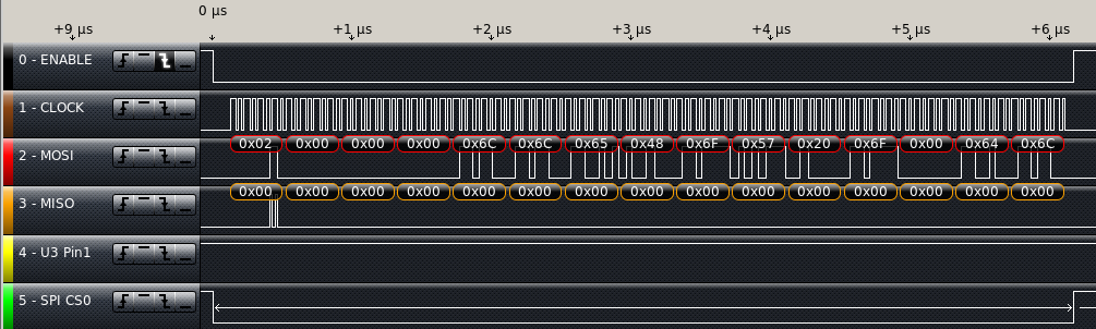
After fixing my typos, I compiled and loaded the code.  The system booted without hanging. then I hooked up the logic analyzer to look for the data being transferred and it didn’t work. The Chip select line(U3 Pin1 ) doesn’t go low for a frame of data.  This means the chip never gets selected to write to.

With several hours of tinkering, I finally have it close, but it is still not working correctly.  The CS0 pin is being activated when the HSPI CS pin is being activated.  So I am getting the correct sequence of bytes when HSPI CS is low, but CS0 is low at the same time.

HSPI almost working

I have not posted a new copy of the software, I don’t believe it is useful to anyone yet.  It isn’t even useful to learn from.

Have you had similar frustrations? Have you gotten the HSPI to work in overlap mode?

Please leave a comment below.


ESP-12E pinout differences

A while ago, I found an e-book about the 8266.  It’s called “Kolban’s book on ESP8266” by Neil Kolban.  He compiled a lot of information on the ESP8266.  I decided to look at this book to see if it has any useful information concerning the HSPI.  It has very little to say about HSPI.  The book lists the API calls without any detail.  What is important is it lists a GitHub repository that has very easy to read example code.  The author of the example code also has a blog with a very good description of how to use the SPI registers.

Since I have the HSPI working with one byte, I decided to try to get the Overlap mode working before trying to add functionality.  I retested with the code from last week and got the same results. Let’s hear it for consistency!  Then I put the call to hspi_overlap_init() in my code just before the sending of data.  Without changing which pins the logic analyzer is attached to, I expect to see chip select to go low and but not see any clock or data, they should move to the other pins.  The data didn’t change pins.  I connected to the SPI bus to see if the data is being sent on both buses.  I checked what should be the clk line and got what looks like data. Next I checked what should be the MOSI line and it looks like the CLK line should look. I created the table below while doing the testing.  I did find that data was on both sets of pins.

Pin#(expected) — Most likely signal
PIN10(MISO) — ?
PIN11(IO2) — ?
PIN12(CLK) — ?
PIN13(IO3) — MOSI
PIN14(MOSI) — CLK

I grabbed the first build of the board to see if it acted the same. I soldered component leads to each of the SPI signals I was interested in and then attached the logic analyzer to those pins as I needed.  With the old board it looks like MOSI is on Pin13 and CLK is on Pin12.  There are definitely different pinouts of the ESP12E from (I assume) different manufacturers.  This could be a problem if I go to any kind of mass production.  There is a newer version of the chip ESP-12F that seems to match the pinout of the chip I currently have.  I don’t see any evidence on the web of different pinouts of the 12F yet.  This needs more research.

I will have to change the layout again but I can test the HSPI with RAM by cutting the traces and putting jumpers in to correctly wire the chip.  I went back and modified the schematics to reflect these changes.  Since the pinout for the 12F matches the lines I am pretty sure of, I used it to update the schematic.  I changed the labels on the Pins of the chip then changed the connections to the SPI RAM.

SPI Pinout FixESP-12F

Have you had to work with manufactures changing specs on you? Or obsoleting a chip? How did you deal with it?

New PCBs

The PCBs arrived this week.  I really like the way my Logo came out.  20160415BarePCB

I do want to make an adjustment, make the arrows larger, they didn’t even show up on the silkscreen.

PCBLogo

To start testing, I put a jumper in bypassing the lithium cell charger. I then installed the ESP-12E, the SPI RAM, The Crystal, the USB Serial Bridge, the voltage regulator, and the USB connector. Just enough to power up, load a program and test the basics.

20160415assembledPCB

First test was to  connect to PC and run ESPlorer– it worked.

I got a message:


AT-based firmware detected.
AT+GMR
AT version:0.40.0.0(Aug 8 2015 14:45:58)
SDK version:1.3.0
Ai-Thinker Technology Co.,Ltd.
Build:1.3.0.2 Sep 11 2015 11:48:04

I then tried to install my test version of the software and it wouldn’t install.  I went back to ESPlorer and started playing with the DTR and RTS to see what would happen. It turns out I got DTR and RTS backwards. So I cut the traces and added a couple of jumpers. This is the kind of mistake I was hoping to catch in the design review.

It programmed great with the wires swapped. My code crashed, back to a “Hello World” version.

Turns out the internal memory chip installed on the ESP-12E does not run at the settings I had specified with esptool.py.  I found this out by setting it to 20MHz DIO mode which started working. I then switched it to QIO mode to see what happened. QIO worked, next I tried running at 40 MHz. That worked.

../esptool/esptool.py --port /dev/ttyUSB0 --baud 230400 write_flash -ff 40m -fm qio -fs 32m 0x00000 ../bin/eagle.flash.bin 0x40000 ../bin/eagle.irom0text.bin

I enabled HSPI Overlap mode by adding spiRamInit() to the end user_init(). Ran without crashing. When I started building for use, I discovered no SPI Master Read available.  I saw something that looked correct for slave read, so I borrowed a line from it and did a write followed by that line– it built. I uploaded the code, and it ran, still no testing of the SPI Ram.

I added the function calls to write “Hello World” to the SPI RAM. and read back and put out to the console. and I got garbage back to the console.  Not a surprise. Debugging with a logic analyzer next week.

Have you written code for the ESP8266. Have you worked with SPI before? I would love to Hear from you.