SPI RAM

The Esp8266 family have limited ram for both running firmware and for storing data.  To store large blocks of data it makes sense to have external RAM.  Since I want to transfer large blocks of data to program target applications I am adding external ram to the SPI bus.  Microchip makes a 1 Mbit SQI interface serial RAM.

Note: SQI is a version of SPI where the data is read/written 4 bits at a time.

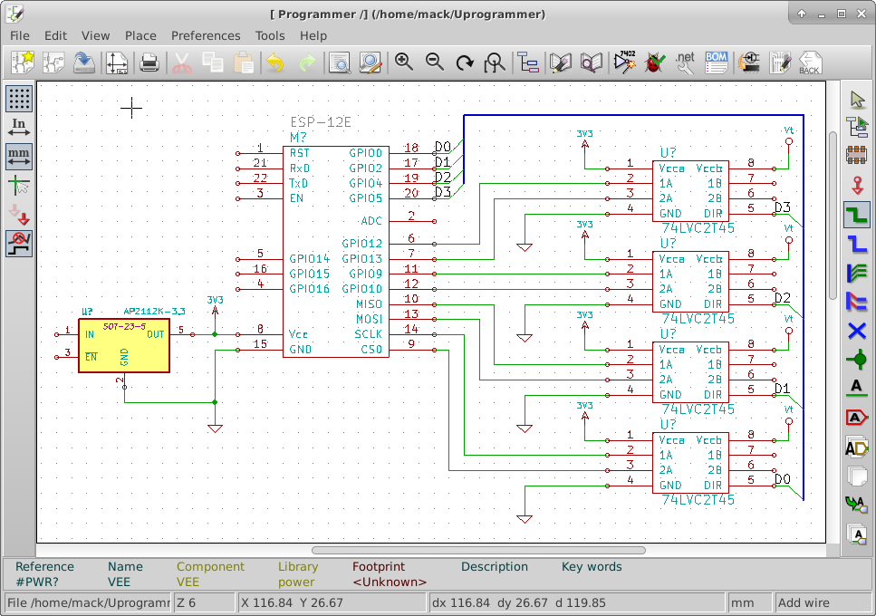
To interface with SQI RAM I had to research how the SPI pins are connected to the flash memory.  I searched on the web for the ESP-12e Flash chip.  The clearest result(not necessarily accurate) is the Winbond W25Q32BV.  I downloaded its datasheet along with a photoplot of the  ESP-12E routing.  I followed the signal traces of each pin  from the Winbond flash chip to the edge of the board.  The following table represents the signals and their pins on the edge of the board.  This is based on very limited understanding of the ESP-12E.

ESP-12E Pin #    Signal    Notes
9                CS        Don't use this, it is chip select for  the flash chip
10               MISO/IO1  Should be available when firmware is loaded into ram
11               IO3       SQI IO Pin
12               IO2       SQI IO Pin
13               MOSI/IO0  Should be available when firmware is loaded into ram
14               SCLK      Clock for all SPI and SQI data

The individual chip select lines determine which device is on the SPI/SQI bus.

This research led me to change the ESP-12E part in the library to reflect the signals, I have added a new chip to the library for the Microchip serial flash and attached the appropriate signals along with GPIO15 for the chip select.

SQI RAM

Initial Connections

As I start connecting signals on the schematic, I look at which pins have dedicated functions.  The dedicated functions I need, I handle first.  This allows me to adjust the rest of the design around the required elements.  To make the schematic easier to read, I try to avoid crossing traces.


I went into the library editor and moved the pins of the ESP-12E around to make it easier to read the schematic.

I have connected the SPI pins from the ESP-12E to the level shifter chips.  I have also connected four GPIO pins to the level shifter chips.   I have placed the 3.3V power connections to each of the level shifter chips and the ESP-12E. I have also tied the 3.3V regulator to the 3.3V power bus. I connected GPIO0, GPIO2, GPIO4, GPIO5 to the direction pins of the level shifter chips.  I have also connected Vt to the level shifter chips. this voltage will come from the target to be programmed.

I have ordered 5 ESP-12E boards from Ebay.  I should receive them within 30 days.  Once I receive them, I will start doing a basic hello world project.

Initial Connections

Programming interface circuitry

The ESP-12E operates on a voltage between 3.0 and 3.5 Volts. The devices that I want this programmer to service could have operational voltages as low at 1.8 Volts and as high as 5 Volts.  Some routers operate on 12 Volts but their programming logic is probably in the 1.8 to 5.5 V range.


I searched for “level shifters” on the web and found a nice option from NXP.  The 74LVC2T45 is a dual supply, two bit Bi-directional buffer.  Maximum propagation delay is 10.1 nS  which would be compatible with JTAG speeds up to about 50 Mbps.  This would allow me to configure the I/O direction of each pair of bits at the connector.

Except for high voltage programming enable pins, These chips should be able to handle all the voltages for programming devices.  I will still have to design the programming enable voltage pins separately.

I am adding this new IC into the custom library and I will place several on the schematic.Interface Circuitry

Schematic Design

The purpose of the schematic design is to organize the design elements in a way that is clear and easy to follow.  The schematic is used to show the electrical connections between components in a circuit.


I opened the schematic.

I placed the ESP-12A and noted the power connections Vcc and GND.  This device requires 3.3 volts operational voltage so I will need a voltage regulator to supply the radio. While looking for more data concerning the  ESP -12E I found a better pin layout and description on ESP8266.com.  On line I have found the part draws 300 mA at peak.

Searching on Digikey, I found a regulator AZ1117CH-3.3 under US $0.09 each in quantities of 4000.  It looked like a very good fit until I looked at dropout voltage.  With a 3.7 V lithium battery for the supply, a dropout voltage greater than 0.4V is too much. Typical dropout voltage for this part is 1.2V.

Note: Dropout voltage is the minimum extra voltage above regulated to maintain regulation. I 3.3V regulator with a 0.5V dropout voltage requires an input voltage of 3.3+0.5 = 3.8V to still be able to regulate to 3.3 Volts.

So I look again, I have used and like the AP7333-33 voltage regulator.  It’s maximum current is 300 mA.  that doesn’t leave any margin.  I keep looking. The next part I find from Digikey is the AP2112K-3.3. It can run at up to 600mA leaving plenty of margin, with a dropout voltage of 0.25 V. The price is under US$0.11 each in quantities of 3000.

I add that to my library and to the schematic. I found a similar SOT23-5 pin part exported it. I then imported it in the the programmer library and edited the part name to match the ordering number.

Schematic 06062015