Interactive Router

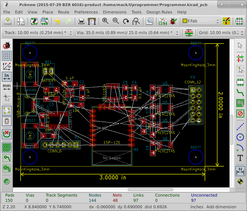
I did the routing this week.  I set up the minimum trace width and separation as specified on OSHpark’s website. White lines show the connections I still needed to make, this is called the ratsnest. When the ratsnest is completely gone, I knew I was finished with the routing.

I started by placing routes on the left side of the board and then working towards the right avoiding power and ground pins. As I worked, I noticed some of the parts did not line up well for routing so I moved some footprints around the board.

About 2/3rds done I found the interactive router feature.  If I switched to OpenGL mode, the interactive router became active.  This router saved me a lot of time compared to the first part of the layout.

Once I finished routing everything except power and ground, I set up a pour area for ground on the back side of the board.  To pour, I had to define a zone on the backside of the board.  I kept this zone at least 15 thousandths from the edge of the PCB to make sure it worked with OSHPark.  I also created an area around the antenna on the ESP12e that has no pour to meet their layout requirements.

To finish a pour, I had to right click on the edge of the created zone, mouse over the zone menu item and then select fill zone.  I connected the surface mount parts to ground by connecting a trace to the SMT pad and then placing a via to connect to the ground plane.  I finished the layout by connecting the positive voltage supply traces. I then filled the ground plane zone again to clean up any adjustments I made to tracks on the board.

Interactive Router

Target Vpp Connections

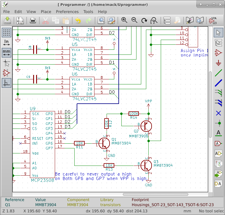
I am finishing up before going to layout.  I implemented the high voltage design last week but wasn’t complete.  I still need to control it going to the target.  I looked at Microchip’s PicKit 3 as a reference design and pretty much copied the controlling transistors for my circuit design.

The drive of the high voltage to the target is turned on by a PNP transistor which is turned on by another NPN transistor.  Grounding of the target Vpp is controlled by another NPN transistor.  These transistors are controlled by GP6 and GP7 of the port expander.

It is important to note that things could get damaged if GP6 and GP7 were both turned on at the same time and the Boost voltage regulator is turned on as well.

I ran the annotation, then the electrical rules check, I got some errors.  It found a bunch of unconnected pins that I hadn’t marked yet. I went back and marked them. I checked each remaining error and they are not really bad, but they needed to be checked anyhow.  Then I ran the netlist tool. I then ran CvPCB to assign footprints to the new parts.

I hit the button to perform automatic footprint association, and I didn’t want to, It re-assigned footprints that I had already chosen.  So I had to go back through the whole list verifying each component.

I finished by arranging the layout by watching the ratsnest as I placed the components in PCBnew. I am now considering this layout Version A, I have a lot of room for revisions.

VPP Control Parts Placement Ver A

Change in Design

I changed my mind, I think the programmer should be able to be reprogramed without any special tools.  This means that the Microchip processor is getting removed and replaced with a USB to serial bridge.  I have decided on the Silicon Labs CP2104 USB to serial bridge. My decision is based on cost and minimal external components. I went to several suppliers and compared 1K quantity prices.  I also confirmed that I can used the built in USB VID and PID.

I followed the example circuit in the datasheet for the CP2104 making minimal connections for a self powered device.  Since I am going to eventually have a battery that is the correct mode to wire for.

Since I no longer have the Microchip processor to control the high voltage, I connected the SET line of the AAT1230 to GPIO15 of the ESP12E.  The pulldown on GPIO15 will keep the voltage regulator disabled during a reset and I will drive it low anytime I am not using it, minimizing the current it draws from the battery.

I connected the Feedback voltage from the high voltage and the target voltage divider into an analog SPDT switch(NC7SB3157 chip) and connected the common terminal to the ADC input of the ESP-12E.  This allows me to verify what voltage the target system is at and what Vpp voltage is maintained during programming.  I ran out of IO pins on the ESP-12E, so I am added an SPI port expander(MCP23S08).  I have to give up 1 pin for chip select but I gain 8 general purpose IO pins.  So I moved the data direction control pins to the port expander and then connect GPIO5 to the CS line of the port expander. I verified the port expander could operate at 3.3V to match my operating voltage.

I connected GPIO2 to the Switch select line of the analog switch.  A high selects the VPP voltage divider, a low selects the Target voltage divider.  The voltage dividers are necessary because I could be dealing with more than the 3.3 V that the ESP-12E can handle.

None of the new devices were in the libraries.  I had to create each of the MCP23S08, the CP2104, and the NC7SB3157 in the schematic library.  I still have to connect the Vpp line to the target connector where I can leave it high impedance, set it to high Voltage, or Ground it.

USB Bridge and Vpp Port expander and Analog switch

High Voltage supply

I changed my mind, I am going to add the High voltage supply before I go to layout.

I am going to use a switching boost regulator to give me between 6 an 12 volts to supply to Vpp on the target.  I mentioned a couple of weeks ago that I found a chip to achieve this goal.  I’ll be using the AAT1230. I created the symbol in the library and placed it on the schematic.

I need to research the highest voltages needed for Vpp, I am designing the circuit with a range from 7 to 14V for Vpp.  I am using a simple voltage divider on feedback circuit to set the regulated voltage.  With a threshold of 0.6V the setting resistors need to be calculated as follows R2/(R1+R2) = 0.6/7. From the datasheet R2 is specified at 4.99K. I simplify by inserting the value for R2 and multiplying by 7. The result is 34.93K/(4.99K+R1) = 0.6. I then multiply both sides by 4.99K+R1 to simplify again. Now the equation looks like 34.93K=2.994K+0.6 x R1. I subtract 2.994K from both sides to simplify again I get 31.936K=0.6xR1. I now divide by 0.6 on both sides of the equation and I get 53.23K = R1. To validate the number I go back to the original formula which is the desired voltage(7) times the resistor tied to ground(4.99K ohms) divided by the sum of the resistors(4.99K+53.23K = 58.22K) which has to equal my threshold value of 0.6V.  7×4.99/58.22 = 0.60 (with a little rounding)  Using the programming line I can set Vpp from 7V to 14V output in 16 steps. Each step will be just under 1/2 a volt.

In my experience Vpp is defined as a range.  For the Microchip PIC16F87X series chips the range is 13+0.5V  The output voltage can be set in that range.

I have attached this voltage divider circuit to the analog inputs of the microchip USB chip  this will allow me to check if we are getting good voltage out of the regulator.  I am also using the microchip chip to set the voltage.  If I hold the set line low for longer than 500 μS the regulator will reset down to the 7V setting. If I pulse it low for less than 500 μS it will increment up the steps.

I also tied a voltage divide to Vt to measure target voltage as well.

Sorry for all the math, but as an engineer sometimes it’s unavoidable.

Boost Regulator

Initial Placement

This week I upgraded to a new build of KiCad. I followed the link on KiCad EDA to get the build script here.  This install script took just a few seconds to download and more than an hour to complete.  It asked me to confirm several package installations.  It went on to download the source code, libraries, and documentation for the current version of KiCad.  The version I am now developing in is 2015-07-29 BZR 6016.  This version gets footprint libraries from github.com and caches them on your machine.  This is great but it has some drawbacks.  Several parts had to be re-connected on the schematic.


I had to re-assign footprints to the components.  To get to the CvPCB program you have to run it from eeschema. There is a toolbar button and it’s in the tools menu.

Once I finished with CvPCB, I loaded the PCB new program from the KiCad project manager. I clicked on the netlist button. I clicked on read current netlist and then close.  The components were in a jumbled mess in the upper left corner of the layout sheet.

I selected all the footprints and drug them to the center of the sheet.  Because I don’t have a form factor I am trying to fit, I am optimizing layout for minimal board space used. (this will cost the least)

I got the board down to 3″ x 1.5″  without any standoffs.  I decided to size it up to 3″ x 2″ to make room for standoffs and modifications. I then rearranged for this new space. I tried to manage data flow from left to right across the board.  I also tried to keep the antenna away from any components.FirstLayout