Making, Hacking, and or Engineering.

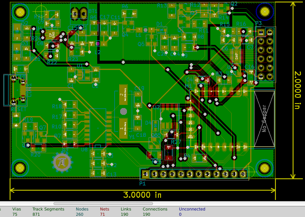
I am waiting for PCBs to come in and hardware testing is next on my agenda for the design. So, I wanted to explore the differences of Making, Hacking, and Engineering.

Dictionary.com Definitions:

Making:

1. the act of a person or thing that makes:

The making of a violin requires great skill.

Hacking:

8. Informal. to make use of a tip, trick, or efficient method for doing or managing (something): to hack a classic recipe;

to hack your weekend with healthy habits.

Engineering:
1. the art or science of making practical application of the knowledge of pure sciences, as physics or chemistry, as in the construction of engines, bridges, buildings, mines, ships, and chemical plants.
I of course picked the definitions relevant to this blog. Making requires skill but doesn’t necessarily have to be clever.  Hacking as used in the term “life hack” are clever or unusual ways of doing something efficiently.  Then finally Engineering is applying known science to a given goal. As an electronics designer, you are usually working in a blend of all three ways.
A few days ago, I did a little project that was basically all Making.  I wanted an inline set of controls for a wired headset that I already own. I looked up the requirements online, designed the schematic, and PCB layout and ordered PCBs.  I really didn’t do much engineering and it wasn’t particularly clever.
When designing something that has never been done before, Engineering is great, but sometimes falls flat. Perhaps the design hasn’t been done because no one has found a clever solution yet. An engineer has to be careful when they incorporate a hack into their design.  Often clever solutions have unforeseen drawbacks that may not become apparent until thousands of units have been produced.
Sometimes a design hasn’t been done because no one has seen the need for it before.  This is often a nearly pure engineering process. Nothing in the design is hard to do, but you have to know the science(or it’s shortcuts) to complete the design.
Side note: In some cultures Engineering is about individual and public safety. An Engineer’s job is to make sure a product or design won’t hurt someone. Although I think it is important to always be thinking about safety in your design, this is not part of this discussion.
Side Note: Scientific shortcuts speed up the design process.  For instance we know the left hand rule for figuring out the magnetic polarity of a coil given it’s direction of current flow.
Do you have any favorite science shortcuts? Are you a maker, a hacker, or an engineer?  Is there another way to look at creating something that you’d like to talk about?

Happy Pi day again

This is the second time this blog has passed by March 14th.  I am kind of a math geek, so it’s fun for me to celebrate.  And of course I chose PI as the symbol for this blog and my business.

I ordered PCBs and components this week. I selected Blue solder mask with white silkscreen from DF Robot, I chose 1.6mm board thickness, and ten boards. This costs US $26.95. The parts from digikey cost US $25.66 + shipping. keeping this iteration of the design’s material costs to under US $60 — not bad.

V00F DFRobot

I also registered my Business name (Prototype Iteration) with the state of Oregon this week.

I see that there are about 300 views of this blog each month. Are any of you in a similar stage of developing a project?  Are you ordering PCBs and components?  I look forward to hearing from you.

Preparing for fabrication and population Hardware V00F

This week is about getting the files ready for ordering.  I thought about calling it Sometimes you have to do boring stuff II.  I’ve pushed an update to github so that fabrication files and the new BOM are available to download.

I started by running a BOM file from PCBnew.  I gave it a different name so that I could compare with the Last BOM. I opened the V00B file and then the new file called programmerV00F.  I set them up so I could see the differences.  There might be a good merge tool, but I don’t know of it.  Line by line I started going through the components.  Adding, removing, or updating each one. I deleted the lines that represented things that did not need to be ordered. This included the battery, mounting holes, and my logo. Once the obvious items had been taken care of, I went through it line by line and took counted my inventory of each item to make sure I had enough components to build one board.

I wrote the reference designator on each component bag as I went through the BOM.  This will save me time as I populate the PCB.  I found R5 in the BOM and I remembered I still need to experiment with it’s value, so I will pull it from a resistor kit. I skipped the charge indicator LEDs and their limiting resistors, I am not sure I want them yet. I changed my mind, I decided to get 5 each of the green and LEDs and I will use resistors out of my Resistor kit.

V00FDcartI ran the fabrication files to get gerber formatted layout files and the numerical drill file. I overwrote the older files because I knew that they were stored in a zip file. I then packaged them into a new zip file named UprogrammerV00F.zip.  I did a quick review of the output files, and I am ready to order.

I’d love to hear what your thoughts are on this design.

Parts Placement (Hardware V00E)

With the design review and testing done, it is time to update the layout.  I started by doing a Design rules check on the schematic. I got 3 errors, two were passives connected to inputs.  I changed the analog input of U10 Pin 3 to a passive pin. This is not a problem, but might be in other circuits. The third indicated two power outputs were connected together.  The CH340G has a 3 volt pin that operates as either a power input (3.3v operation), or as an output (5v Operation), I went in and edited it to be a bidirectional pin.  It still gave me a warning, but it’s acceptable.

Design rule warnings and errors are important, for each one, I will check to make sure it doesn’t represent a real problem and try to fix it.

I then ran CvPCB to confirm all devices have an assigned footprint.  I had made some changes that means a few new components, and footprints. I got all the parts assigned and saved them. then saved the schematic sheet. I then ran a netlist. I opened the layout design, and imported the new netlist… it gave me an error. It couldn’t find the library Housings_SOT-23_SOT-143_TSOT-6. The library name had changed, I went back into CvPCB and found the TO_SOT_Packages_SMD library that had the SOT23 footprint that I needed for all of my transistors. After making reassigning the footprints, I re-saved CvPCB and the schematic file, then generated a new netlist.

This left me with a bunch of parts all jumbled together. I started by spreading them out so I could see their ratsnest better. Once I saw how much components needed to be moved around, I ripped up all traces as well as the ground plane.  This gives me the freedom to re-arrange the board more efficiently.  My strategy was to start at each end of the board and work to the middle.

Looking at the design, the switch for upload takes up a lot of space and is not needed. I went back into the schematic and removed the upload switch. This required that I generate a new netlist and read it into PCBnew.

I left the USB connector where it was, put the Lithium cell in the NW corner, the Reset circuit in the SW corner, the wifi module in the SE corner, The test header along the south edge, the target connector on the NE corner and the high voltage circuit along the north edge.

PartsPlacementV00E

I routed the board using the interactive router. I then added my logo on to the board. I want to edit my logo a little bit, I may change that before I send the files off to fabrication.

FinishedLayoutV00E

The kicad files are on www.github.com, use the link just below my logo to download them.

Do you have any comments, would you do something differently,  can you see a better placement of parts?