A while ago, I found an e-book about the 8266. It’s called “Kolban’s book on ESP8266” by Neil Kolban. He compiled a lot of information on the ESP8266. I decided to look at this book to see if it has any useful information concerning the HSPI. It has very little to say about HSPI. The book lists the API calls without any detail. What is important is it lists a GitHub repository that has very easy to read example code. The author of the example code also has a blog with a very good description of how to use the SPI registers.
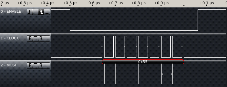
Since I have the HSPI working with one byte, I decided to try to get the Overlap mode working before trying to add functionality. I retested with the code from last week and got the same results. Let’s hear it for consistency! Then I put the call to hspi_overlap_init() in my code just before the sending of data. Without changing which pins the logic analyzer is attached to, I expect to see chip select to go low and but not see any clock or data, they should move to the other pins. The data didn’t change pins. I connected to the SPI bus to see if the data is being sent on both buses. I checked what should be the clk line and got what looks like data. Next I checked what should be the MOSI line and it looks like the CLK line should look. I created the table below while doing the testing. I did find that data was on both sets of pins.
Pin#(expected) — Most likely signal
PIN10(MISO) — ?
PIN11(IO2) — ?
PIN12(CLK) — ?
PIN13(IO3) — MOSI
PIN14(MOSI) — CLK
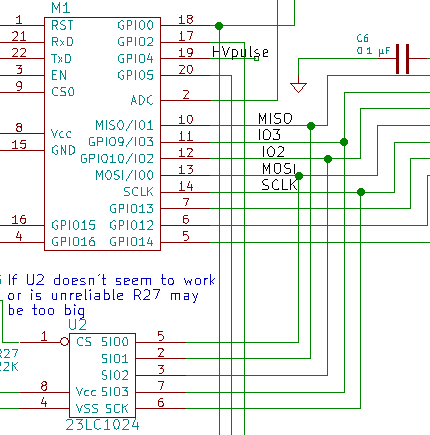
I grabbed the first build of the board to see if it acted the same. I soldered component leads to each of the SPI signals I was interested in and then attached the logic analyzer to those pins as I needed. With the old board it looks like MOSI is on Pin13 and CLK is on Pin12. There are definitely different pinouts of the ESP12E from (I assume) different manufacturers. This could be a problem if I go to any kind of mass production. There is a newer version of the chip ESP-12F that seems to match the pinout of the chip I currently have. I don’t see any evidence on the web of different pinouts of the 12F yet. This needs more research.
I will have to change the layout again but I can test the HSPI with RAM by cutting the traces and putting jumpers in to correctly wire the chip. I went back and modified the schematics to reflect these changes. Since the pinout for the 12F matches the lines I am pretty sure of, I used it to update the schematic. I changed the labels on the Pins of the chip then changed the connections to the SPI RAM.

Have you had to work with manufactures changing specs on you? Or obsoleting a chip? How did you deal with it?