Cost review

Newest SDK:

Espressif has moved the SDK to GitHub.  At this point, It is version 2.1.  I have no indication that they have done anything with the ADC Feature I requested.  I have not updated to this newest SDK yet. I will do that before I spend any time working on firmware.

New component costing:

The 74LVC2T45 level shifter chips are US $0.32 each in low quantities.  The PCA9306 I2C level shifter are about US $0.60 each in low quantities.  This results in the costs of the level shift components arount $1.50.  The original single part costs around US $1.25 each in low quantities.  This is not a big difference in cost but it does affect board space.

Design review:

Continue reading

Modifying the circuit for better Vpp control

Planning:

I needed finer control of Vpp.  Since this is an experimental design, I decided to make some calculated guesses to choose the right values.

To start with, I believe that putting a resistor between the emitter and ground of the feedback transistor will limit the gain of the transistor.  The voltage of this resistor will rise as the current through it increases limiting the current gain of the circuit.  The first guess I tried was calculating the resistor as if the transistor wasn’t there(same as fully saturated) for my max voltage (25 V).

Continue reading

Cutting in the Vpp prototype

I opened my design schematic and realized I had already designed the Vpp control design. So now I have two options. I used an inductor in the first design to filter the base current of the voltage divider.  In the second design, I just used an RC low pass filter to filter the base current of the transistor.  This project has gone long enough that I am forgetting details of things I have already done.

Prototype Choice:

I prefer the design I did last week to the earlier design. If I find the system doesn’t regulate very well, I may incorporate parts of the earlier design.

Cut in Planning:

Looking at the last schematic and schematic where I want to end up, I can see I need to remove Q4, 5, R6 and R9. I then need to attach pin 1 of the FAN5331 to Pulse. Pin 2 to GND, Pin 3 to Vps. Pin 4 and 5 to the supply side of L1. Short Q4 Pin2 to 3. Finally replace R9 with a transistor with filter to HVPulse.

Continue reading

Vpp Regulation test

Second Thoughts:

I am having second thoughts about co-processor model.  This significantly increases the complexity of the firmware for this design.  I haven’t ruled out any options yet.  If I can get a good voltage for Vpp without the co-processor, I may decide to go back to the level shifter.

Programmatically controlling Vpp:

I have been thinking about how to make an “adjustable voltage” switching regulator adjustable by the microcontroller.  By putting a transistor on the low side of the voltage divider feedback, I believe I can have linear control of the generated voltage controlled by the Sigma-Delta output. I got a basic circuit design from the FAN5331 datasheet. I then replaced the ground side resistor of the feedback voltage divider with an NPN transistor.  I came up with the circuit below.

The FAN5331 has a 1.25 volt reference comparator to decide if it needs to generate more voltage or wait.  With the Sigma Delta input to r3 at 0 out of 255, the transistor will never turn on and the voltage on the feedback will be above the 1.25V threshold and the regulator will effectively shut down.

Resistor Calculations:

Continue reading

Refactoring

Update:

No new information on the ADC feature request on Espressif”s forums.

Side Project:

I have started layout of the SSD1332 Breakout PCB.  I finished the layout and ordered PCBs from OSHPark.  Based on the datasheet for the SSD1332, I can get significantly better performance by using it in one of the 8 bit bus modes.  Someone suggested that I look at STM32 processors to drive the display with.  I will be considering that option this week.

Better Firmware:

Continue reading

Vpp Control Loop (Firmware V00M)

Plan:

This week I decided to work on the control loop. I decided to add a simple adjustment scheme to the 5 mS system timer event. And then create a way to change the required voltage in increments of 0.1 Volts starting at 10.0

Implementation:

I created a local “static” variable in the events.c file for the target voltage. I then created a function to set this variable target_voltage and another function to get the value of target_voltage.  I then added a simple if statement into the 5ms event that increments the duty cycle of the Sigma Delta if the measured value is too low and decrements it otherwise.  I compiled and tried this, Vpp is ugly.

pic_42_3 Continue reading

Vpp regulation (Firmware V00K)

Update

Neither the PCBs or components have arrived yet.

The decision

This week I decided to work on the Vpp feedback loop. I am interested to see how well the system can regulate the boosted voltage operating on an interrupt driven control loop.

Testing

I needed to see if I could get reliable numbers back from the ADC while generating a given voltage.  First step then was to make it so I could change the state of the analog switch from the serial console.  I used the keys ‘<‘ and ‘>’ to select which input I would be connected to the ADC. I wasn’t sure which signal would be connected to the ADC, So I made sure I could select each one individually. Typing < into the console sets GPIO15 to low and typing > sets GPIO15 high. While setting this up, I discovered that GPIO2 wasn’t configured correctly like I had thought.  I fixed this and added the little bit of code to give me control and tried it.  It built and uploaded without a hitch.

Failure

The code was running, ready to test. I hooked up my oscilloscope to watch the output of the Vpp pin to compare to the analog readings.  When first hooked up, the scope was reading 4.8V and the ADC gave me a result of 15. (ADC should give a result of approximately 230.) I hit the > to see and I got a result of 24.  (off by a factor of 10).  I decided to see if that would hold. I played with the Sigma delta till I got an output around 10 volts. I landed at 10.8V.  At this voltage, the ADC result was 24(no change).  This was disappointing. I hit the < key and read out the ADC with result of 20. Not what I was looking for. (expected something either twice the original value of 15 or 512)  The results are not what I had expected(fail).

Diagnostics

Continue reading

Good Enough

Designing anything new rarely goes as expected.  Of course you try to design as much as possible using technology and designs you are already familiar with.
I was working with a monopole wire antenna this week.  I needed to tune and impedance match the antenna to be as efficient as possible between 905 and 930 MHz.

The tool I had available to do this tuning with is a Spectrum analyzer with a built in Tracking Generator and an external return loss bridge.

Note: For optimal transfer of energy from a transmitter to an antenna, they have to have the same impedance.  Most rf transmitters are designed with an output impedance of 50 Ohms. This means that the most efficient antenna will have a characteristic impedance of 50 Ohms. The characteristic impedance of an antenna depends on it’s length and it’s surroundings.

When the impedance doesn’t match, a matching network is needed to fill in the gap.  If an antenna looks more like a capacitor than an inductor, then a series inductor can be used to make up the difference.  If the antenna looks more like an inductor, then a series capacitor can bring it back to close to 50 Ohms.  Of course the series inductor or capacitor will burn a little energy but most will get transfered to the antenna.

The antenna I worked on this week tuned fairly easily around 860 MHz.  When I cut the antenna shorter for 915 MHz, it became very hard to tune.  My job would have been a lot easier if I had a network analyzer that operated in the 900 MHz Range.  An analyzer would have told me the characteristic impedance of the antenna as well as whether it was more inductive or capacitive.

I didn’t have the a network analyzer and was under a time and budget constraint. My solution was to put different inductors in series and see if that would work. It worked great at 860 MHz. It didn’t work at 915 MHz.  My next idea was to put a capacitor in series, the only capacitor I had that would fit on the PCB was a 0.1uF.  This would be too high of a value of reactance to be useful.

My next idea was to put an inductor to ground to reduce the inductive reactance of the antenna.  This produced mediocre results.  I could only get about 85% efficiency from the antenna in the 900 MHz Band.  I tried successively larger values looking for the best return loss.(most emitted energy).

I had to settle for “Good Enough”. If I get the chance, I would like to go back and buy a capacitor kit that will let me try the series capacitors.  The antenna will work well, but the overall range of the radio will a little bit smaller.

Have you had to settle for good enough?  What are your thoughts about how “Perfect is the enemy of good”?

Code Documentation Firmware V00J

I Know that my code is very poorly documented.  So I want to focus on organizing and documenting the code.  To start with, I started looking for online classes that teach documenting code.

I found very little about commenting code.  I did find an interesting article I need to think about a bit more. The general theme of this article is to write code in such a way that comments should be rare.  For instance, code should probably be re-written if it needs comments to explain it. Variables should be named in a way that describes what they contain.

I was just about to give up searching. I was thinking I would start by putting header comments before each function or method.  This article gives pretty good reasoning not to do that. So this week, I decided to look at just one file — user_main.c.  Git does line by line version control.  I decided on one small header block at the beginning of the file.  This header block will indicate the license, original author, and/or the template source.

I looked to the header comments to know what to pass to and get back from a given function.  I have decided to make a new document that describes in better detail how to use each function.  This new file will be called UprogrammerFunctions.txt.  Since I removed the Comment block from in front of user_rf_cal_sector_set, That is the first function I am documenting in the API.

There is a big block of code in user_init() that all it does is set up the IOs to their initial states.  I copied that code into a new function called setup_io_pins() at the end of the user_main.c file. Next, I deleted all the test code I had commented out.  Finally, I made a couple of macros in user_config.h called VOLTAGE_BOOST_ENABLE()  and another one called VOLTAGE_BOOST_DISABLE()

Note: My definition of a macro is the use of a symbolic reference to represent other code.  In this place, I am using VOLTAGE_BOOST_ENABLE()  to represent  gpio16_output_set(0) to make it a little more clear what is going on. I also created a function in wifi.c to set up the wifi modem called wifi_init() and also put a prototype of wifi.init() in wifi.h.  I then moved the two wifi calls out of user_init() into the function wifi_init().

I tried to build and the call to the new function setup_io_pins() caused a linker error.  I needed to create a prototype of this function. I put it in user_config.h and it compiled, I uploaded it and it ran just like before I started cleaning up the code. I believe my user_main.c file is much more readable now.  I have uploaded the new version to GitHub. Click the firmware link in the right column of this page to go look at it or download it.

I would like to hear about your experiences cleaning up and commenting code.  What are your preferences for commenting code.

Component analysis (Hardware V00G)

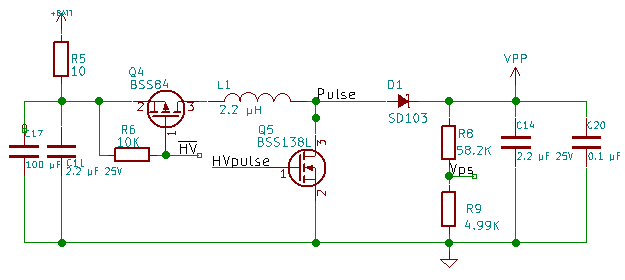
Last week, the voltage boost circuit would barely get above 12 volts.  This would work for most devices but I had set my goal at around 20v. I rechecked datasheets to verify I wasn’t operating out of specification.

Diode D1: The voltage across this diode is really close to 12V when Q5 is on and C14 is charged. From the datasheet, the reverse breakdown voltage(Vr) for and SD103 is 40 V.  This is a fast switching Schottky diode. This is probably not my problem.

FET Q5: The voltage across the drain to source will also reach around 13 Volts when in the off phase of the pulse stream.  The drain to source breakdown voltage is 50 V. This transistor can switch fast enough even at 80MHz.  This is probably not my problem.

Resistor R5: I chose to use 100 Ohms when I populated the PCB.  I am definitely seeing a voltage drop at C17 when driving to around 12 Volts.  If this is the problem, I will not even be able to get to 12V when running on the lithium cell. I think this is causing the problem.

To test this, I decided to change the resistor to 47 Ohms and redo my testing.

I tested with a prescaler of 0, 1, 2, and 4.  With a prescaler of 4 I got 20 volts with the duty set to 51.

Analysis and testing revealed that the filter resistor R5 was too much resistance.  By changing it’s value to 47 Ohms, I was able to get the circuit operating the way I wanted.

I made no changes to the software other than changing the prescaler.  For this firmware, that is a value that I expect to be played with, so no firmware upload this week.  I did change the value of resistor R5 to 47 Ohms.  So I uploaded a new version of the hardware to GitHub.

I would like to see smaller steps between voltages, I am thinking of changing the inductor to a smaller value to improve efficiency and control.  I am not sure this works, but it might be worth a try.

I am still working in an area of electronics I don’t understand very well.  This is the first time for me to design a switching voltage boost circuit.  Do you have any suggestions of how to do it better? How about stories about your own experience with switching power supplies.