
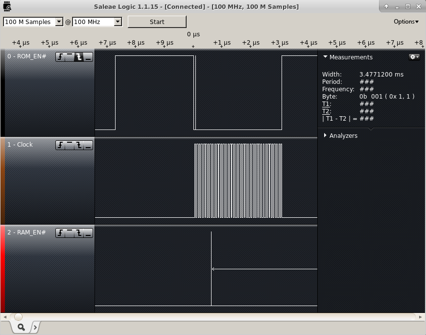
The SPI RAM was still unproven. I want to test it before I do a new layout. I checked the SPI lines with a Saleae Logic16 which unfortunately can only sample 3 lines at 100MHz I was concerned that the SPI RAM would be on the SPI bus at the same time as the FLASH. This could occur anytime the CS0 and the HSPI CS were low at the same time while the processor was writing or reading from the flash. So I connected to the two chip select lines and the SPI clock line. I triggered capturing off of the first falling edge of CS0.
I configured GPIO15 to HSPICS at the beginning of user_init and it appeared to not make any difference. I then changed it to a digital pin and set it high and still didn’t appear to make a difference. So I guessed something I was initializing was causing it to change back to the mode it had been in before. I set the Pin to a Digital output and set it high at the end of user_init, and it worked. Since that worked, I tried changing the last step in user_init to set up the SPI overlap configuration. This also works. It looks like that for about 300 ms there is bus contention between the SPI RAM and the FLASH memories. This has got to be solved before I go to a new layout.
What I need is to keep the SPI RAM CS line high anytime the FLASH CS is low but follow GPIO15 the rest of the time. It’s helpful to look at in a truth table.
GPIO9  | GPIO15 | SPI RAM
 CS0   | HSPICS |    CS
--------------------------
   0   |    0   |    1
   0   |    1   |    1
   1   |    0   |    0
   1   |    1   |    1
There is only one zero in the table, this means it can be represented as an or gate. If I invert CS0 and or the signals together I would get the results I want. I figured out a circuit that would work that just adds a transistor, a diode, and a couple resistors. A PNP transistor to pull the line up when CS0 is low and a diode to block the current when GPIO15 is driven low at the same time that the RAM CS is pulled high. There will have to be a pulldown resistor to make sure the CS will go low when it needs to.
I have pushed these minor firmware changes to github.

