Update layout Hardware V00I

Finally time to update the layout.  The charging circuit works well and I changed the level shifter on the schematic last week. So this week, I updated the layout.

I started by generating a new netlist. Next, I ran CvPCB to verify all the parts had footprints associated with them. They all do. Next I ran PCBnew and imported the netlist; making sure the exchange footprint settins was set to change.  I got an error:

Error: Component 'U3' pad '~' not found in footprint 'Housings_SSOP:TSSOP-20_4.4x6.5mm_Pitch0.65mm'

I had to figure out what that means before moving on.  It suggest one of the pins was named wrong either in the schematic symbol or the footprint library. I checked the schematic symbol first. I noticed the GND pin didn’t have a pin number assigned to it. Easy fix, added it and updated the library. I set the GND pin number to 11, saved it to the library, made sure it was in the schematic correctly, and re-generated the netlist.  I had to delete it and re-place it into the schematic to correct the schematic.  This meant that CvPCB no longer knew the footprint to use, so I updated it and re-generated the netlist again. No more errors in PCBnew import of the netlist.

I started by ripping up the unconnected traces. Then I started placing footprints.  I hid the bottom layer to make it easier to see what I was working around on the top layer.  Once I had the parts placed, I started routing traces.  I had to adjust component placement a few times to get everything to fit.  As I got to a point that I couldn’t do all the traces on the top side of the board, I un-hid the bottom layer.  While I was working with both sides, I had to re-fill the zones several times to correct for the areas I added new traces on the bottom side.

I finally got to 0 unconnected nets. I did a quick look to make sure all the references were readable and not under other parts.

layoutv00i

I plotted out the Gerber files and did a quick check to see if it looked OK and got ready to order.  When I look at Gerbers, I am looking for broken traces and unintentionally connected traces.  I used Gerbview to do this check. As I went into Gerbview and tried to load the files, the were double of all the files.  It looks like the developers of KiCad decided to change the naming conventions  for output to gerber.  I went in and deleted all the files in that folder and re-ran the plots.  While looking at the gerber files, C10 and U3 references were covered up.  I went in and fixed them and re-plotted.  While I was at it, I discovered U10 wasn’t anywhere near it’s footprint.

I created a zip file with the plot files ready to upload to a fabrication house. I have uploaded the files to the github repository, click the hardware link in the right column to go get it.

Are you using Kicad?  What tools are you using to design in?  Do you have trouble finding datasheets for Chinese parts?

Lithium Charger Testing (Hardware V00I)

I installed the Lithium cell charger chip and it’s associated components.  While I was soldering the components, I noticed that R5 wasn’t soldered correctly.  This is the current limiting resistor for the voltage boost circuit.  So I need to retest the boost circuit.

I then attached the cell and the radio led blinked once.(with no connection, this was expected)  I connected the USB from my computer into the circuit and D2 (Red) lit up. This is STAT1 signal from the charger IC. From Table 5 in the AAT3672 datasheet STAT1 on by itself indicates the system is fast charging the lithium cell.  I disconnected the Cell with the USB still connected, both D3 and D2 blinked until I reconnected the lithium cell and the system then went back to fast charge.

I grabbed my DMM and checked some voltages:

From USB: 4.65V (A Little low, but I have connected the Uprogrammer to a long USB cable for convenience)
Output to Board: 4.65 V (Matches input voltage)
Lithium Cell: 3.96 V (Good range for Fast Charge)

These voltages make sense, I am very happy with these results.  I waited a while to check the results again.  While I was waiting, I started doing some testing of the Voltage Boost Circuit.  With Just the boost circuit turned on, I measured 4.64 Volts on Vpp.  I checked the Duty and prescaler and they were set to 0 and 4 respectively.

I then set the duty cycle  and measured the voltage at Vpp

20% : 19.6 Volts
30% : 20.8 Volts
40%: 21.8 Volts
50%: 22.6 Volts

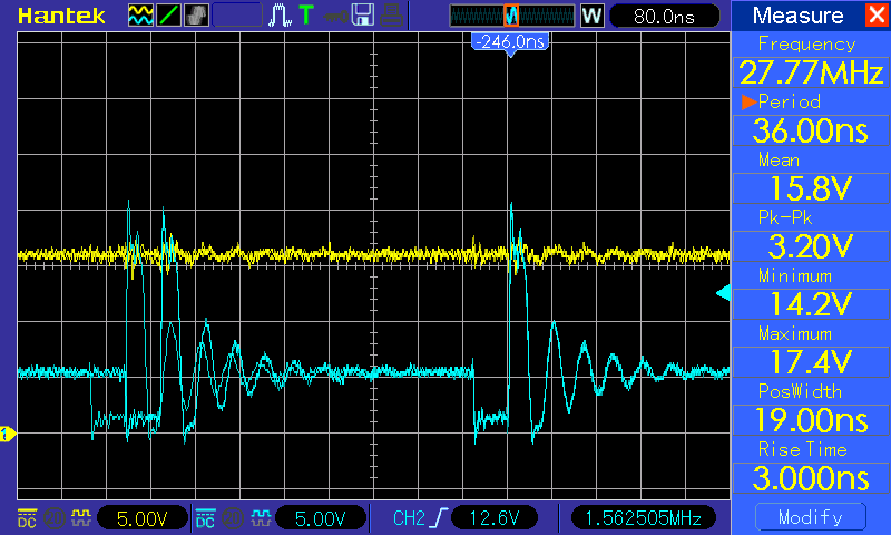
I played with the prescaler and the highest voltage I got was 24 Volts at 50% duty cycle and prescaler set to 9.  This is beyond design specification and has the potential to cause damage to the circuit, I don’t expect to do this in the future. I am happy to know that I have some margin in the design to if I need 20 Volts. I took the following image from my oscilloscope with a Prescaler of 4 and a duty cycle of 10% (25).

pre4duty25

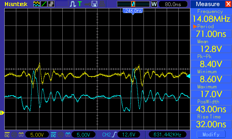
I am not happy with the large steps setting the output voltage of the boost circuit.  I decided to load the circuit with a 10 K Resistor to see how it affected the output voltage.  I soldered a 1206 10K Resistor on top of C20. This lowered the output voltage for 10% with a prescaler of 4 down to 12.8 Volts  But the best voltage I could get out of the system was 18 Volts.  This also made Vpp a lot noisier(See scope image below), I want to add some more filtering.

pre4duty25w10k

I added a resistor to the schematic parallel to C20 and also a place for another capacitor.  The resistor I set the value to 20K as a starting point and the capacitor I set to 1 uF.  The 20 K resistor will draw less current and that should reduce the noise.  The capacitor will also reduce the noise and provide a larger reservoir for current changes when programming a target device.

After doing all this testing the lithium cell voltage was at 4.12 V. This is near a complete charge, I expected the system to go to complete charge very soon. This is indicated by the Green LED being on alone.

After it switched to charge complete, I grabbed my DMM and checked some voltages:

From USB: 5.05V (Minimal current draw so no Voltage drop through the USB cable)
Output to Board: 5.05 V (Still matches input voltage)
Lithium Cell: 4.19 V (4.2 Volts is maximum charge voltage for individual LiPo Cells)

The charging circuit is working as expected.  I disconnected the USB and the LEDs turned off. I re-connected the USB and the Red LED came on for a few minutes and then it went back to only the green LED on.

I have uploaded the updated schematic to GitHub, click the hardware link in the right hand column to go get it.

Do you have a circuit you want to test before layout? Do you have a design you are tinkering with?

Component analysis (Hardware V00G)

Last week, the voltage boost circuit would barely get above 12 volts.  This would work for most devices but I had set my goal at around 20v. I rechecked datasheets to verify I wasn’t operating out of specification.

Diode D1: The voltage across this diode is really close to 12V when Q5 is on and C14 is charged. From the datasheet, the reverse breakdown voltage(Vr) for and SD103 is 40 V.  This is a fast switching Schottky diode. This is probably not my problem.

FET Q5: The voltage across the drain to source will also reach around 13 Volts when in the off phase of the pulse stream.  The drain to source breakdown voltage is 50 V. This transistor can switch fast enough even at 80MHz.  This is probably not my problem.

Resistor R5: I chose to use 100 Ohms when I populated the PCB.  I am definitely seeing a voltage drop at C17 when driving to around 12 Volts.  If this is the problem, I will not even be able to get to 12V when running on the lithium cell. I think this is causing the problem.

To test this, I decided to change the resistor to 47 Ohms and redo my testing.

I tested with a prescaler of 0, 1, 2, and 4.  With a prescaler of 4 I got 20 volts with the duty set to 51.

Analysis and testing revealed that the filter resistor R5 was too much resistance.  By changing it’s value to 47 Ohms, I was able to get the circuit operating the way I wanted.

I made no changes to the software other than changing the prescaler.  For this firmware, that is a value that I expect to be played with, so no firmware upload this week.  I did change the value of resistor R5 to 47 Ohms.  So I uploaded a new version of the hardware to GitHub.

I would like to see smaller steps between voltages, I am thinking of changing the inductor to a smaller value to improve efficiency and control.  I am not sure this works, but it might be worth a try.

I am still working in an area of electronics I don’t understand very well.  This is the first time for me to design a switching voltage boost circuit.  Do you have any suggestions of how to do it better? How about stories about your own experience with switching power supplies.

Sigma Delta still causes reboots Firmware Version 00E

I was hoping but not expecting the SDK Update to fix the Sigma Delta problem.  So first thing I did this week was to test.  Same failure as before.  I had two Ideas this week that might be an answer to the problem.  On another project, I was using the Arduino IDE to develop a little weather station project.  In it, I was using old code that set certain pins as output.  Those pins were/are tied to the SPI bus and was causing it to reboot.  Maybe, there is a pin set to have Sigma Delta(ΣΔ) output that is also tied to a critical pin.  My second thought is that if the ΣΔ is causing interrupts, I should disable them.

A good practice for microcontroller programming is to always set up all I/Os immediately after a reset.  I have gotten sloppy and haven’t done that with this project. If a pin is connected to the ΣΔ that shouldn’t be, this will fix that.
I started by writing down what each pin will do in the design. I referred to the schematic for each pin.

Pin 18 GPIO0 -- Output -- controls analog switch
Pin 22 GPIO1 -- Output -- TxD0
Pin 17 GPIO2 -- Output -- sets VPP output high
Pin 21 GPIO3 -- Input -- RxD0
Pin 19 GPIO4 -- Output -- ΣΔ pulse stream to generate Vpp
Pin 20 GPIO5 -- Output -- Sets Vpp output low
Pin 14 GPIO6 -- Output -- SCLK (SPI and HSPI overlap) (need to verify Pin number for ESP12F)
Pin 10 GPIO7 -- BiDir -- MISO (SPI and HSPI overlap) (need to verify Pin number for ESP12F)
Pin 13 GPIO8 -- BiDir -- MOSI (SPI and HSPI overlap) (need to verify Pin number for ESP12F)
Pin 11 GPIO9 -- BiDir -- QIO2 (SPI and HSPI overlap) (need to verify Pin number for ESP12F)
Pin 12 GPIO10 -- BiDir -- QIO3 (SPI and HSPI overlap) (need to verify Pin number for ESP12F)
Pin 9 GPIO11 -- Output -- CS0 (SPI) (need to verify Pin number for ESP12F)
GPIO12 -- BiDir  -- Data to target device
GPIO13 -- BiDir  -- Data to target device
GPIO14 -- BiDir  -- Data to target device
GPIO15 -- Output -- Chip Select for HSPI
GPIO16 -- Output -- Disables Vpp generation

I went into the user_init() function and removed all the commented out code leaving an example of the PIN_FUNC_SELECT() macro. I then set GPIO_PIN0 – 15 registers to 0 which disables interrupts and disconnects the ΣΔ output.  I compiled the code and uploaded it and it crashed.  To find the new problem I caused, I commented out all the new code except setting the GPIO registers to 0. I rebuilt and uploaded the code and … a continuous stream of reboots.  I commented out setting the GPIO registers to 0 then put the PIN_FUNC_SELECT() back in. And … reboots slowly.

I removed the function selects that should be controlled by the API anyhow(GPIO6-11). And … I found a typo on the GPIO6 function select. I fixed the typo, rebuilt, uploaded and it ran at least as well as last week.  I then started testing to see if it fixed the ΣΔ issue. The reset problem still exists.

Next I set a subset of the GPIO registers to a value of 0  I decided to go with the first 8 to see what would happen. Same failure, a stream of reboots. Then I noticed I wasn’t writing to the correct register locations.   I fixed this and then recompiled, uploaded, and code is running, but ΣΔ is still causing a reboot if i set the prescaler to greater than 99.

Next I started looking at the ΣΔ interrupt structure.  Unfortunately it has very little documentation that I have found so far.  I used google to search for articles pertaining to the use of the Sigma Delta and found very little.  My next step is to do a little experimentation. I decided to disable the ΣΔ while changing the prescaler.  I got the same results.  It’s time to make a Hello World program for a sanity check. It would be the minimum to set up and test functionality of the ΣΔ on GPIO4.  If it works correctly, then I have to take a deeper look at my code, if it doesn’t, I’ll have something to post to Espressif’s forum for help.

Have you had similar problems with a chip you have never used before?  I have uploaded the current code to GitHub. Use the link at the top of the right hand column to get the download.

Preparing for fabrication and population Hardware V00F

This week is about getting the files ready for ordering.  I thought about calling it Sometimes you have to do boring stuff II.  I’ve pushed an update to github so that fabrication files and the new BOM are available to download.

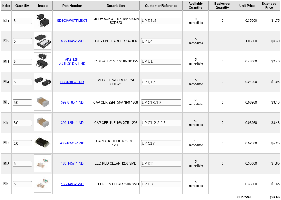
I started by running a BOM file from PCBnew.  I gave it a different name so that I could compare with the Last BOM. I opened the V00B file and then the new file called programmerV00F.  I set them up so I could see the differences.  There might be a good merge tool, but I don’t know of it.  Line by line I started going through the components.  Adding, removing, or updating each one. I deleted the lines that represented things that did not need to be ordered. This included the battery, mounting holes, and my logo. Once the obvious items had been taken care of, I went through it line by line and took counted my inventory of each item to make sure I had enough components to build one board.

I wrote the reference designator on each component bag as I went through the BOM.  This will save me time as I populate the PCB.  I found R5 in the BOM and I remembered I still need to experiment with it’s value, so I will pull it from a resistor kit. I skipped the charge indicator LEDs and their limiting resistors, I am not sure I want them yet. I changed my mind, I decided to get 5 each of the green and LEDs and I will use resistors out of my Resistor kit.

V00FDcartI ran the fabrication files to get gerber formatted layout files and the numerical drill file. I overwrote the older files because I knew that they were stored in a zip file. I then packaged them into a new zip file named UprogrammerV00F.zip.  I did a quick review of the output files, and I am ready to order.

I’d love to hear what your thoughts are on this design.

TAPR Open Hardware License (OHL)

The TAPR Open Hardware License (OHL) is the only license I am considering that is written specifically for hardware and patent law.  It requires that any derivative works be licensed the same.  It requires distribution of all modified works to include the originals unmodified.


This license restricts what a developer can do with the design.  I am hoping that this product has enough value to developers that they would contribute to the design.  With that premise, I would not like other developers to be limited significantly on how they can use the intellectual property.

I am going to use the MIT license for both hardware and software.  I don’t need patent/copyright protection on this product.  Liability protection is a good thing, I intend this product to be “hackable”. Anything submitted to this blog for product design will be considered under the MIT license unless noted otherwise.

Creative Commons

There are several flavors of the Creative Commons license.  I am going to look at the attribution and attribution share alike licenses.

Both licenses are very similar to the modified BSD license and are more explicit about what rights are conveyed by the license. Both require attribution to the author without endorsement from the author.

The share alike requires any derivative works be licensed with the same license or a compatible one.


For this project, I don’t see any advantage this gives me for the final product.  I hope to build and sell these programmers, but if someone else does for a decent price, I would still benefit.

I have to pick a license or make it public domain or someone else could license or patent it in a way that would restrict me or anybody else from building and selling it.

I am applying common design principals in this project. I do not believe there will be anything unique enough to patent.

Modified BSD license for Hardware

The Modified BSD license is pretty much the same as the MIT license plus it prohibits using the name of the copyright holder for promotion.

I am getting most of my information about these licenses from here.


For myself, I don’t care if someone uses my name for promotion.  This license doesn’t help me over the MIT license.

If someone else submits designs, or software to the project, they may use this license without any conflict with the MIT license.

MIT License applied to hardware

The MIT license gives a lot of freedom to developers to use the intellectual property in any way they want.  This includes manufacturing, selling, and modifying the design. It does not require or restrict attribution. It does give the designer some protection for liability.  This is not compatible with more restrictive licenses.


The reasons I want to design this product include:

  • Teaching about electronics design
  • Create a low cost universal In Circuit Chip programmer

If some company picks up this design and produces it at a fair price then both objectives are met. This would create a well documented hackable device for a very reasonable price.

The MIT license for software and hardware is compatible with my goals.

If I want to integrate some other design with more a restrictive license, I would have to switch to the more restrictive license or separate the other design into a module or in the case of software a library.

I will continue to look at other software and hardware licenses.