Javascript

Merry Christmas!

The PCBs came in today, they look great.  Of course I will need to make the modifications I mentioned last week.  I haven’t received the CH340G chips yet. I will wait until I receive them before I start building.

Rev00BPCBs

This week, I wanted to add  a slider to set the Sigma Delta output that drives the voltage booster to the web interface.  I didn’t know javascript at all so, I went to an online tutorial at Codecademy.com. This tutorial is very basic and even explains the basic concepts of programming in general.  I didn’t learn enough to set up a slider, I did learn enough to do some testing.

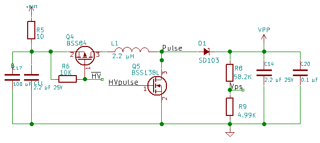
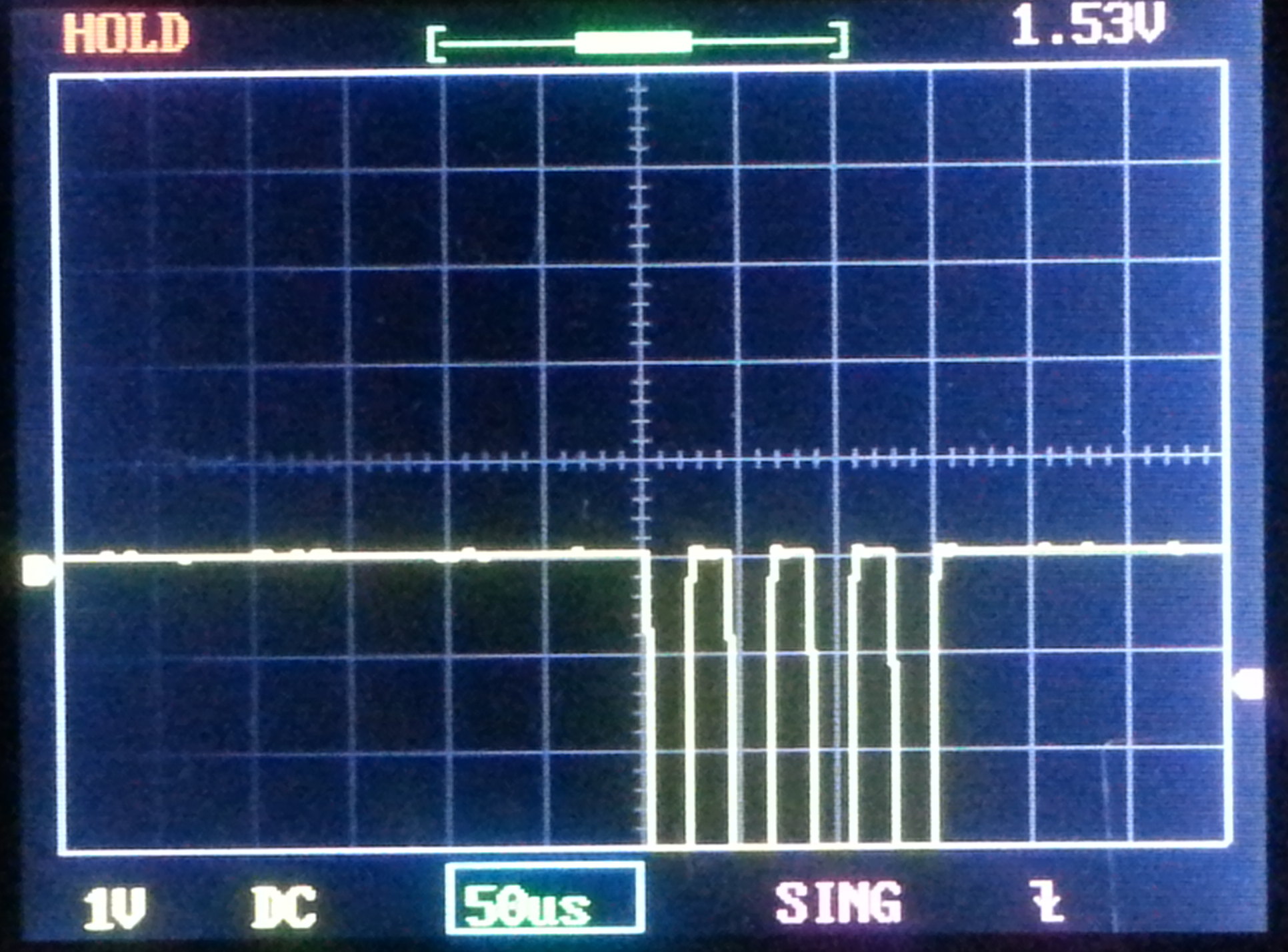
I quickly got the Sigma Delta output working in GPIO12 by copying the necessary code from the test project I was using. I then added a call to config_sigma_delta() from user_init() in user_main.c.  I also added a call to set_sigma_delta_duty() from my test code in cgi_relay.c.  Of course I added includes to sigma_delta.h in both of those files.  I then changed the Sigma Delta output from GPIO12 to GPIO4 to match the HV_pulse line used to run the switched coil.

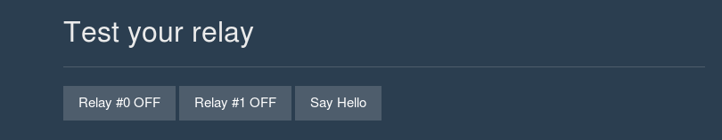
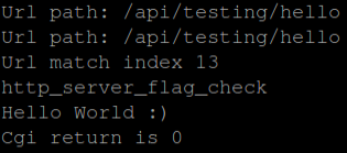
Now if I hit the say Hello button, It changes the Sigma Delta output duty cycle. also, the Chart on the index.html page gives the current reading from the ADC once every 5 seconds.

ADCandSDelta


Web Server feature customization

I found out why my URLs without .html on the end weren’t being handled the same as the rest.  There is an array defined in app.c that maps URL paths to alternate paths.

URLsI haven’t found the code that uses this yet, but it seems pretty straight forward what this is used for.

In the function init_http_server in app.c I found several functions that I think I don’t want.  I put a // at the beginning of those lines so that the compiler treats those lines of code as comments.  This is called “commenting out”.  This is useful when removing code that you suspect has an error, or , as in this case, I suspect I can remove.

I don’t need the captive portal. I am happy if users can use the IP address to get to the web server.  Having a domain name and using the web server from within a local network complicates things.

I commented out the lines:

    http_server_bind_domain(INTERFACE_DOMAIN);
    http_server_enable_captive_portal();
and
    http_server_bind_urls((http_server_url *)&api_urls);

I compiled with these changes, “crossed my fingers”, and uploaded. And… I got a continuous stream of reboots with messages coming into the serial terminal program at 115,200.  this means it started the code that initializes the UART and failed some time after that.

Backing up, I uncommented the server_bind lines and again tested on my board. I am able to connect to the Access Point with my android phone. When I point my phone browser to 192.168.4.1, I get an empty page. When I point my desktop browser to the assigned network address, I also get a blank page from the server.  When I point either browser to smart.relay.com. they both load the initial webpage.

I decided to do a hello world cgi function trying to understand how things work.  To the api_urls I added an entry pointing to a new function called http_tst_api_hello.  I then added that function to the cgirelay.c and cgirelay.h files.  The new function will send “Hello World” out on the serial port using the DBG macro.  The new button shows up on the page, but doesn’t appear to do anything except cause a jump to the top of the page.

I don’t know Javascript, CSS and only a little bit of HTML, this part is going to be a challenge. I did finally get what I was trying to do.  Seems like a small step, but it took a lot of studying and tinkering.

I am not putting any of this code up on github, because I am only taking steps to learn how things work. When I start building in real functionality, then I will start putting this code on github.

Web Page Hello World

Serial Hello World

First web page

I have the web server up and running which is great.

While reviewing my design, I found a few mistakes in the layout.  These mistakes are easily fixed with either a jumper wire or solder bridge, so I can keep on testing when the new PCBs arrive.

The web server isn’t working as easily as I had hoped.  I made a copy of the cats web page in the project, added my banner photo from this site and added html links in each page to point to the new page. With my picture added, It wouldn’t compile.  I am sure there is enough room in ROM, so I just need to figure out some settings. I removed the picture from the project and it compiles. I added an entry in my hosts file to point to smart.relay.com. When I go to smart.relay.com on my network it seems to work most of the time.  Speed and reliability will need to be worked on.

My new page unfortunately comes up blank. If I add .html to the end of the url my page loads correctly.  I went through the pages and added the .html ending to each link.  I don’t understand why this is happening this way.

I opened and modified the eagle.app.v6.ld  I changed the irom_0_seg  line. I changed the len value from 0x51000 to 0x80000.  This allowed me to add the banner photo into the project.  I don’t know if this can cause problems.  Assuming the value was at 0x51000 for a reason gives me reason to be concerned about it.  It’s possible that I have allowed data to overlap which could cause major problems. I need to learn how the .ld linker files work.

FirstWebpage

Web Server firmware

I am waiting on the stuff I ordered last week.  The CH340G chips are probably going to take the longest at 3 to 4 weeks.

To start with I updated my virtual machine to keep it current, I downloaded V1.5.0 of the Espressif SDK, and updated the lubuntu inside of the virtual machine.

I spent this week trying to get the chip running as a web server.  On the ESP8266 forum I found about a project called esp-ginx.  It is a web server with a lot of features.  For me it looks like a lot more than I need.  This is good for this design, I can cut away or ignore the features that I won’t be using or needed.

I downloaded the zip from github.  I ran make from the wrong directory and it failed to compile.  Finally realizing I need to run make from the project directory I was able to get it to compile without any errors.  I then uploaded it to my board and it didn’t work.  I was continuously getting fatal exception (0) on the serial port at 74800 baud.  Thinking that my RAM chip might be causing problems, I decided to remove it and try again.  Still no success.

I then tried to load the code into the NodeMCU board that I also use for testing. I got the same results with it.  I re-loaded my code into my board and got it back to working.  After many tries I finally realized tried putting the app folder in my home directory without any of the SDK files and it compiled.  I loaded this to my board with the commands: make clean, make html, make, and make flash.  The virtual machine had crashed and I needed to reboot my whole system before this worked for me.

This has been very frustrating just to find out that I didn’t understand the way to set up my files.  After I got the web server up and running, I added an entry to my hosts file on my computer.  I made an entry that pointed to he ip address of the board and associated it with smart.relay.com.

SmartRelay

Sometimes you have to do boring stuff

Time to order PCBs and components.

I started by running a BOM in PCBnew.  This lists all the components used on the design.  I imported this into LibraOffice Calc. I then deleted items that don’t have an actual part associated with them. This included mounting holes, the battery, the pushbutton switch, Reset, and the test header. I then sorted on the Reference designators.  I then looked at the old BOM to see what I had already ordered, since I had only used one set of them already.

I ended up with eleven components that I do not already have for the next build. I went to Digikey and added them to my cart for another build of boards.  This will mean I have a mismatch of quantities in the future builds.  I find this acceptable because I may use the leftover parts on another prototype.  I ordered the parts from Digikey. That left the CH340G USB to Serial bridge and the PCBs.

I ordered ten pieces of the CH340G off of Ebay for US $3.68 and I ordered ten PCBs from DFRobot for US$26.95. To order the PCBs i had to plot the gerber files and put them in a zip file and email it to DFRobot’s manufacturing service.

This is not the most fun part of a project but necessary.  As the project progresses, I’ll have to start tracking my inventory as well.

Digikey order V00b

Re-Layout Update V00B

Now that the design review is complete, I am updating the PCB layout.

I started by going into CvPCB to check and fix any components. I feel that the pad sizes are too large with the Handsoldering footprints.  I changed all 1206 Handsoldering footprints to 1206 standard  footprints. The 1×12 connector hasn’t been assigned yet, I chose a 0.100″ pin header footprint which I will leave empty. The Socket Strip 1×12 fit my needs.

While doing some research, I found a chip to replace the level shifter chips I was using.  The FXMA108 chip by Fairchild Semi does all 8 bits with automatic direction changing.  It’s capable of up to 80 Mb/s.  It allows me to simplify my design and remove the shift register.  Each buffer automatically shifts direction based on how its pins are being driven.  I removed the four level shifter chips and replaced them with this one chip. I had to create the chip in my library.

While moving parts around the layout, PCBnew shut down unexpectedly and I lost about 2 hours worth of work. There are so many changes to this layout that I decided to remove all of the traces and start new.  Under the edit menu is Global Deletions, I selected tracks and hit OK.

I moved the microUSB connector to hang off of the edge of the PCB and changed the slotted holes to round with the longest dimension used for the diameter of the circle. I moved the component values outside of the board boundary which helped remove some clutter from the board.

I started laying out the traces around the level shifter first because that section is straight forward.  Ikepth the schematic open so i could make quick changes on the schematic to simplify the layout. With each change I madeon the schematic, I would generate a new netlist and then read it into PCBnew. I made many component placement adjustments while routing the traces. I finished by doing a fill of the ground plane on the bottum side of the board.  This made a couple of unconnected nets stand out so I fixed them.Re-Layout V00B


Design Review V00B

Design reviews should be done often, at least just before a new design goes to fabrication.

During testing I had wished for some test pins at the edge of the PCB for verification. I want to add and label test pins for Reset, Txd, Rxd, 3.3V, SCK, MOSI, MISO, IO2, IO3 and L1 pulse.

I added these testpoints to the schematic along with a ground that’s easy to get to. I am putting them into a through hole 1×12 connector. I moved P1 test into the same header. In layout, I’ll place this connector next to the edge where I can get a clip lead connected for testing.

USB to Uart chip completely changed, copied reference design from NodeMCU design. It’s helpful to look at a second design for a sanity check. Everything matches up to an Arduino clone schematic found on the web.  I had left DCD, RI, DSR, and CTS unconnected.  Leaving inputs unconnected can cause problems.  These connections may have internal pullups/pulldowns but I couldn’t find any reference to that in the datasheet. Each of these lines indicates data is ready to flow when held low, I put pulldowns on each of them.

I had changed the SPI connections to correct the mistakes I had made earlier, I have gone back to verify these connections and found conflicting information. I traced the gerber image I had found to get the pinout I currently have. If it’s not correct, I will have the test pins to help me figure out the  correct pinout.

I had replace the port expander with a shift register still using the SPI to fill the register. According to the datasheet, the data shifted in will be latched on the rising edge of the RCLK pin.  If I treat RCLK as a Chip Select Pin on the SPI, a one byte write will set all of the outputs very quickly. This appears that it will work well.

The VPP circuit changes are a big gamble. I don’t know if it will work.  I am adding a 0.1 µF capacitor to the output to reduce output noise.  I am adding a 10 Ohm resistor and a 100 µF capacitor to filter noise from getting back into the rest of the system. I need to isolate the ground of the high voltage circuit to only connect to regular GND Net at only 1 place on the layout. This will help reduce noise transfer back into the rest of the system. The design update is on GitHub, use the link in the upper right hand of the page.

V00BVPPCircuit

Updating Schematic V00B

In the last few posts, I found several problems with the design as well as found some ways to reduce Bill of Material costs.  I also want to make soldering of the parts easier for a hobbyist.

I had problems using the CH340G chip on my NodeMCU board.  I couldn’t find any references to this problem on the internet.  So I replaced U8 (the CP2104 USB to UART bridge) with the CH340G USB to UART bridge.  I inverted DTR and RTS  and connected them to GPIO0 and RST respectively.  Using transistors as the inverters means that when U8 is not powered, it won’t draw those two lines down.  This is looking forward to when the design is battery powered.

I used the NodeMCU schematic as reference during this part of the design since it is close to what I want to do with this part of the design.

I changed the reset push-button switch to pads on the board and left the upload push-button switch unchanged but don’t plan on installing it unless I run into problems programming the board.

I also want to make things smaller, U9 is a large part of the board.  A shift register can do the same thing and be less expensive. I found the 74HC595 to replace U9. I am still clocking data in using the SPI bus, and then latching it with a pulse from GPIO5.

For the High voltage, I removed the AAT1230 and replaced it with two logic level FETs. One to disable the circuit to drop current draw when in low power mode connected to GPIO14. The other the pulse stream that generates the current through the inductor connected to GPIO4.  This means all the pins on the module are used up again.

Kicad schematic and layout can now be found here. The pcb layout is not current to the schematic, I still need to do a design review before I start the layout.

UProgrammerSchV00B

ADC and PWM V00D

I have implemented the Reading the ADC from a keystroke (R) sent over serial. I have implemented the PWM on GPIO12.  My initial testing of the PWM has a lot of jitter and didn’t perform at the frequency I configured.  I want to set up a Hardware PWM and see how it performs.  Jitter and frequency can be important when running a switching power supply, so I want to get this right. I set GPIO2 high to select Target voltage as the input to the ADC and set a variable power supply at 0.3 volts tested it and got results around 300, then set it to 0.5 volts and got ADC results around 500 indicating it’s working as expected.

The chip doesn’t have a PWM instead it has a built in sigma-delta pulse generator.  It creates a stream of pulses to achieve the specified duty cycle by adding more pulses to fill in the middle. The chip will connect the sigma delta generator to any GPIO pin I choose.  I can use any free pin to drive the boost inductor switch. If I optimize the inductor for the width of the pulse, I should get very efficient voltage conversion.

There is no API configured for the Sigma Delta unit.  I had to write directly to the registers that set the pin connection and the Sigma Delta unit.  I had to do a lot of experimentation to understand how to set up the Sigma Delta pulse generator.  There is a piece of example code on Espressif’s forum that doesn’t work correctly, but gave me the information I needed to figure out how to configure the unit.  The example code tries to be very generic, and my code is over-simplified for testing.

SigmaDelta

Functions added to test Hardware GPIO and Boost Regulator

I  have three things left to test before I re-layout the board.  The high voltage generation and the io channels, and the ADC/Analog Switch.  Since I have to control an IO pin to change the voltage output of the boost regulator, I will effectively be testing both together. I Soldered the inductor, diode, and feedback resistors on to the PCB. I will do the analog testing next week.

I start by adding a new command to the simple serial menu.  Since we are changing voltage I think tapping V is a good choice to increment the Voltage value.  First thing to do is set GPIO15 as an output and drive it low(Reset the Voltage Boost regulator). When the system displays the menu, then I set GPIO15 to a high value.  This will allows me to check the status of the pin with a volt meter. I expect it to be near zero V for about 1 second then about 3.3Vafter that until I can implement the next step.  I confirmed these values proving the gpio capabilities are working as expected. Now I should also be seeing about 6V at the test point on the output of the boost regulator. I did not see any voltage at the test point.

I need to figure out what is wrong with the voltage regulator, first, I am going back to the datasheet to verify I know how to set the voltage level. I inspected really closely and found that pin 12 of U7 did not take solder when I added the chip to the board.  With no connection on pin 12, no voltage could get to the inductor.  To fix this, I overflowed pins 10, 11, and 12, then used solder wick to remove the excess.  This still took several tries.  With the chip soldered correctly, I am now getting 7.7 volts about 1 second after I connect power to the board.

I added the V command to the parser to step this voltage. I managed to damage the boost regulator during testing. I am looking remove this regulator and implement one using the PWM. This choice will reduce the cost as well as simplify the PCB design.

Since I damaged the regulator, I decided to test the GPIO functions on an IO that wasn’t connected to anything at the moment. I chose GPIO12.  I added a command in the simple serial menu that sends a stream of 4 low pulses approximately 20 microseconds wide and separated by 20 microseconds. I chose 20 and 20 because I have a kit oscilloscope that has a 200KHz bandwidth that I wanted to test with.

I want to test PWM capability next week as well.  I have updated the code on GitHub.

GPIO12