Re-Layout Update V00B

Now that the design review is complete, I am updating the PCB layout.

I started by going into CvPCB to check and fix any components. I feel that the pad sizes are too large with the Handsoldering footprints.  I changed all 1206 Handsoldering footprints to 1206 standard  footprints. The 1×12 connector hasn’t been assigned yet, I chose a 0.100″ pin header footprint which I will leave empty. The Socket Strip 1×12 fit my needs.

While doing some research, I found a chip to replace the level shifter chips I was using.  The FXMA108 chip by Fairchild Semi does all 8 bits with automatic direction changing.  It’s capable of up to 80 Mb/s.  It allows me to simplify my design and remove the shift register.  Each buffer automatically shifts direction based on how its pins are being driven.  I removed the four level shifter chips and replaced them with this one chip. I had to create the chip in my library.

While moving parts around the layout, PCBnew shut down unexpectedly and I lost about 2 hours worth of work. There are so many changes to this layout that I decided to remove all of the traces and start new.  Under the edit menu is Global Deletions, I selected tracks and hit OK.

I moved the microUSB connector to hang off of the edge of the PCB and changed the slotted holes to round with the longest dimension used for the diameter of the circle. I moved the component values outside of the board boundary which helped remove some clutter from the board.

I started laying out the traces around the level shifter first because that section is straight forward.  Ikepth the schematic open so i could make quick changes on the schematic to simplify the layout. With each change I madeon the schematic, I would generate a new netlist and then read it into PCBnew. I made many component placement adjustments while routing the traces. I finished by doing a fill of the ground plane on the bottum side of the board.  This made a couple of unconnected nets stand out so I fixed them.Re-Layout V00B


Design Review V00B

Design reviews should be done often, at least just before a new design goes to fabrication.

During testing I had wished for some test pins at the edge of the PCB for verification. I want to add and label test pins for Reset, Txd, Rxd, 3.3V, SCK, MOSI, MISO, IO2, IO3 and L1 pulse.

I added these testpoints to the schematic along with a ground that’s easy to get to. I am putting them into a through hole 1×12 connector. I moved P1 test into the same header. In layout, I’ll place this connector next to the edge where I can get a clip lead connected for testing.

USB to Uart chip completely changed, copied reference design from NodeMCU design. It’s helpful to look at a second design for a sanity check. Everything matches up to an Arduino clone schematic found on the web.  I had left DCD, RI, DSR, and CTS unconnected.  Leaving inputs unconnected can cause problems.  These connections may have internal pullups/pulldowns but I couldn’t find any reference to that in the datasheet. Each of these lines indicates data is ready to flow when held low, I put pulldowns on each of them.

I had changed the SPI connections to correct the mistakes I had made earlier, I have gone back to verify these connections and found conflicting information. I traced the gerber image I had found to get the pinout I currently have. If it’s not correct, I will have the test pins to help me figure out the  correct pinout.

I had replace the port expander with a shift register still using the SPI to fill the register. According to the datasheet, the data shifted in will be latched on the rising edge of the RCLK pin.  If I treat RCLK as a Chip Select Pin on the SPI, a one byte write will set all of the outputs very quickly. This appears that it will work well.

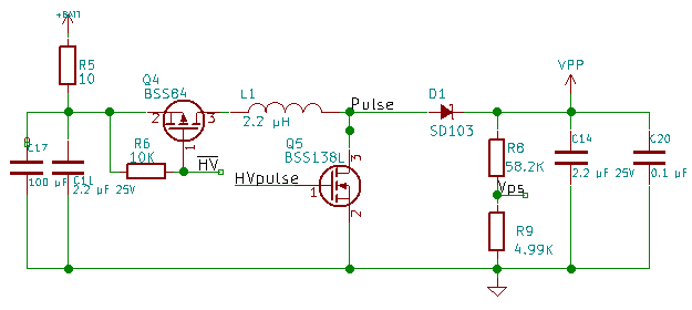
The VPP circuit changes are a big gamble. I don’t know if it will work.  I am adding a 0.1 µF capacitor to the output to reduce output noise.  I am adding a 10 Ohm resistor and a 100 µF capacitor to filter noise from getting back into the rest of the system. I need to isolate the ground of the high voltage circuit to only connect to regular GND Net at only 1 place on the layout. This will help reduce noise transfer back into the rest of the system. The design update is on GitHub, use the link in the upper right hand of the page.

V00BVPPCircuit

External RAM

I found a big mistake.  The pinout I had used for the design has the SPI pinout wrong.  This means that the External RAM and the Port expander will not work until I fix this issue.  So, I found an online layout image that shows the flash chip as well as the pins.  I used esptool.py to request the flash ID.  The Flash ID manufacturer code is C8 and the device code is 4016.  Using Google, I found this to be the GD25Q32 made by GigaDevice.  This is a 4MByte spi/qspi flash chip.  I looked up the datasheet and found the following pinout.

1 CS#-------VDD   8
2  SO|     |Hold# 7
3 WP#|     |SCLK  6
4 VSS-------SI    5

CS#.....Active Low Chip Select
SO......Serial Data Output/ IO1 (Quad/Dual IO)
WP#.....Active Low Write Protect/IO2 (QuadIO)
SI......Serial Data Input/IO0 (Quad/DualIO)
SCLK....Serial Data Clock
Hold#...Active Low Hold/IO3 (QuadIO)
VDD/VSS.Power Connections

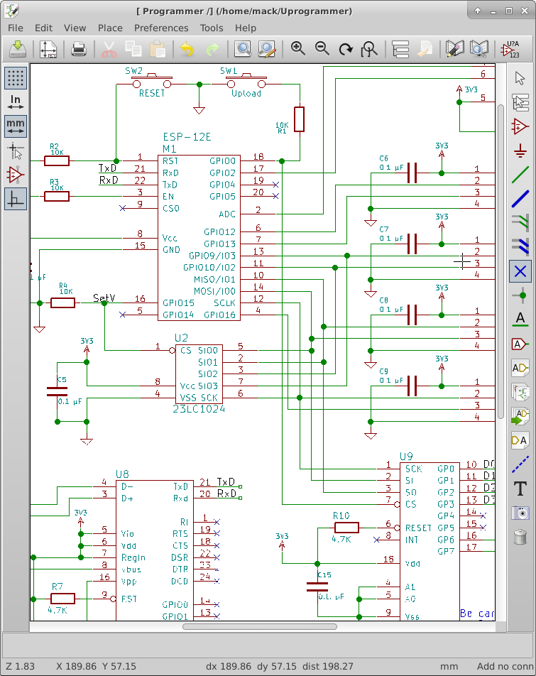
Looking at the ESP-12E Module layout, I found the following connections by tracing the tracks:

Flash CS# is connected to Pin 9 — No Change

Flash SO is connected to Pin 10 — No Change (MISO)

Flash IO2 is connected to Pin 11 — Requires a Change

Flash SI is connected to Pin 14 — Requires a Change (MOSI)

FLash SCLK is connected to Pin 12 — Requires a Change

Flash IO3 is connected to Pin 13 — Requires a Change

I also discovered that if I want to use the Built in SPI Chip selects, I need to use GPIO0(CS2) or GPIO15(HSPI_CS).  TxD is CS1 which is a conflict for testing so I can’t use CS1.  I found this in esp8266 datasheet.

To fix the pinout on the schematic, I went into the library editor and just changed the pin numbers. I left the pin order in place for the schematic.

For the Chip Selects, I connected the RAM CS# to GPIO15(HSPI_CS) and the port expander to GPIO0(CS2).

I have some other schematic changes to make, I am still considering changing to the CH340G USB serial bridge.  The problems that I have had have given me reason to consider not using it.  I may have a faulty chip, I will test with another one, and if the problem goes away, I will feel more confident changing to the less expensive chip.

I have added the SPI and SPI overlay library code to the project source. No functionality has changed, so I am not uploading the code to GitHub yet.

HSPIconnections

Change in Design

I changed my mind, I think the programmer should be able to be reprogramed without any special tools.  This means that the Microchip processor is getting removed and replaced with a USB to serial bridge.  I have decided on the Silicon Labs CP2104 USB to serial bridge. My decision is based on cost and minimal external components. I went to several suppliers and compared 1K quantity prices.  I also confirmed that I can used the built in USB VID and PID.

I followed the example circuit in the datasheet for the CP2104 making minimal connections for a self powered device.  Since I am going to eventually have a battery that is the correct mode to wire for.

Since I no longer have the Microchip processor to control the high voltage, I connected the SET line of the AAT1230 to GPIO15 of the ESP12E.  The pulldown on GPIO15 will keep the voltage regulator disabled during a reset and I will drive it low anytime I am not using it, minimizing the current it draws from the battery.

I connected the Feedback voltage from the high voltage and the target voltage divider into an analog SPDT switch(NC7SB3157 chip) and connected the common terminal to the ADC input of the ESP-12E.  This allows me to verify what voltage the target system is at and what Vpp voltage is maintained during programming.  I ran out of IO pins on the ESP-12E, so I am added an SPI port expander(MCP23S08).  I have to give up 1 pin for chip select but I gain 8 general purpose IO pins.  So I moved the data direction control pins to the port expander and then connect GPIO5 to the CS line of the port expander. I verified the port expander could operate at 3.3V to match my operating voltage.

I connected GPIO2 to the Switch select line of the analog switch.  A high selects the VPP voltage divider, a low selects the Target voltage divider.  The voltage dividers are necessary because I could be dealing with more than the 3.3 V that the ESP-12E can handle.

None of the new devices were in the libraries.  I had to create each of the MCP23S08, the CP2104, and the NC7SB3157 in the schematic library.  I still have to connect the Vpp line to the target connector where I can leave it high impedance, set it to high Voltage, or Ground it.

USB Bridge and Vpp Port expander and Analog switch