High Voltage supply

I changed my mind, I am going to add the High voltage supply before I go to layout.

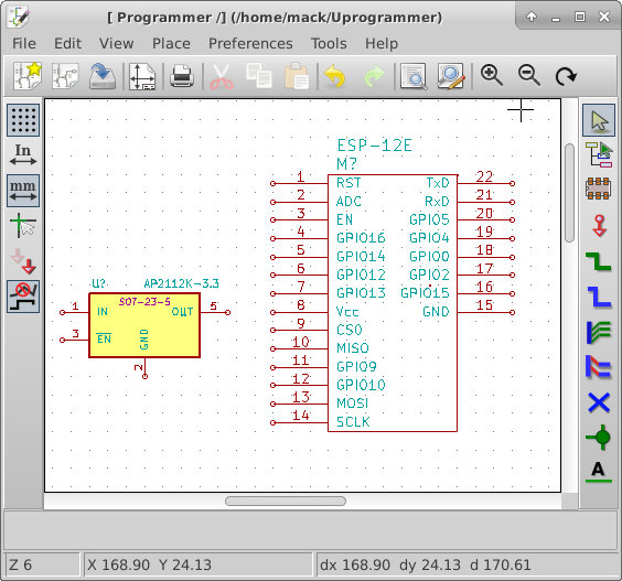
I am going to use a switching boost regulator to give me between 6 an 12 volts to supply to Vpp on the target.  I mentioned a couple of weeks ago that I found a chip to achieve this goal.  I’ll be using the AAT1230. I created the symbol in the library and placed it on the schematic.

I need to research the highest voltages needed for Vpp, I am designing the circuit with a range from 7 to 14V for Vpp.  I am using a simple voltage divider on feedback circuit to set the regulated voltage.  With a threshold of 0.6V the setting resistors need to be calculated as follows R2/(R1+R2) = 0.6/7. From the datasheet R2 is specified at 4.99K. I simplify by inserting the value for R2 and multiplying by 7. The result is 34.93K/(4.99K+R1) = 0.6. I then multiply both sides by 4.99K+R1 to simplify again. Now the equation looks like 34.93K=2.994K+0.6 x R1. I subtract 2.994K from both sides to simplify again I get 31.936K=0.6xR1. I now divide by 0.6 on both sides of the equation and I get 53.23K = R1. To validate the number I go back to the original formula which is the desired voltage(7) times the resistor tied to ground(4.99K ohms) divided by the sum of the resistors(4.99K+53.23K = 58.22K) which has to equal my threshold value of 0.6V.  7×4.99/58.22 = 0.60 (with a little rounding)  Using the programming line I can set Vpp from 7V to 14V output in 16 steps. Each step will be just under 1/2 a volt.

In my experience Vpp is defined as a range.  For the Microchip PIC16F87X series chips the range is 13+0.5V  The output voltage can be set in that range.

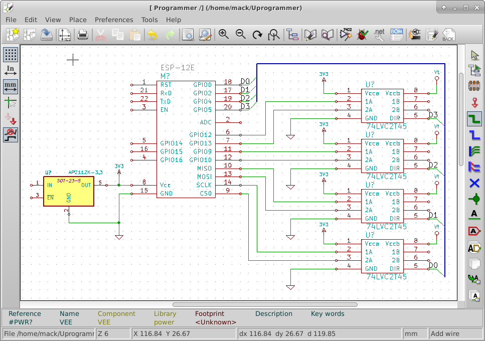
I have attached this voltage divider circuit to the analog inputs of the microchip USB chip  this will allow me to check if we are getting good voltage out of the regulator.  I am also using the microchip chip to set the voltage.  If I hold the set line low for longer than 500 μS the regulator will reset down to the 7V setting. If I pulse it low for less than 500 μS it will increment up the steps.

I also tied a voltage divide to Vt to measure target voltage as well.

Sorry for all the math, but as an engineer sometimes it’s unavoidable.

Boost Regulator

Initial Placement

This week I upgraded to a new build of KiCad. I followed the link on KiCad EDA to get the build script here.  This install script took just a few seconds to download and more than an hour to complete.  It asked me to confirm several package installations.  It went on to download the source code, libraries, and documentation for the current version of KiCad.  The version I am now developing in is 2015-07-29 BZR 6016.  This version gets footprint libraries from github.com and caches them on your machine.  This is great but it has some drawbacks.  Several parts had to be re-connected on the schematic.


I had to re-assign footprints to the components.  To get to the CvPCB program you have to run it from eeschema. There is a toolbar button and it’s in the tools menu.

Once I finished with CvPCB, I loaded the PCB new program from the KiCad project manager. I clicked on the netlist button. I clicked on read current netlist and then close.  The components were in a jumbled mess in the upper left corner of the layout sheet.

I selected all the footprints and drug them to the center of the sheet.  Because I don’t have a form factor I am trying to fit, I am optimizing layout for minimal board space used. (this will cost the least)

I got the board down to 3″ x 1.5″  without any standoffs.  I decided to size it up to 3″ x 2″ to make room for standoffs and modifications. I then rearranged for this new space. I tried to manage data flow from left to right across the board.  I also tried to keep the antenna away from any components.FirstLayout

Associating parts to pinouts

I ran the annotate schematic tool, then ERC to look for obvious mistakes.

I got a bunch of errors because I had left pins unconnected.  This is a reminder that I have to make sure these pins are set to outputs later.  I marked each unconnected pin with a no connect marker and I am down to 3 errors. I replaced the battery connector with a battery symbol.  It didn’t get rid of the error, I will have to check this connection on the netlist.

I then ran the netlist tool with default settings.

Then I ran the CvPCB module of KiCAD. I assigned footprints to the parts from the schematic.  Most of these matched.  For resistors and capacitors, I chose to use 1206 SMD for the footprints.  There is no footprint for the ESP-12E.

I found a footprint online for the module, but KiCAD would not import it. So, I created a footprint and added it to the custom library for the project.

I chose the SW_PUSH_SMALL for the two tactile switches Reset and Upload.  These are through hole footprints, I am thinking I will copy this footprint to the custom library and modify it to go surface mount.

I have only done very simple layouts.  This will be quite a learning experience for me.

CvPCB 1st

Final Connections for first spin

I would like to get the new ESP-12E modules soldered onto a board and start testing.  I have completed the basic schematic.  I added a reset switch, a switch to start in bootloader mode, Decoupling caps.

I moved the PC serial interface chip to a different part of the schematic to make it easier to read.  I added the Net Names TxD and RxD.  I added pull up and pull down resistors to make sure the chip would boot in the right mode.  Searching the web for boot modes showed that GPIO15 has to be pulled low during boot to load firmware. I think I can leave GPIO15 pulled low the rest of the time for normal operation. I also added a connector to the output pins and one for power.

I still want to add battery charging, and a switching boost regulator to generate VPP.  These can be left off at this time so that I can start laying out the board for fabrication.  This would not be normal in an engineering session, the whole design would be complete the first time the boards would be fabricated.

I found a really interesting boost regulator, the Skyworks Solutions AAT1230.  It would make the VPP circuit fairly easy to design.

Note: Decoupling caps are connected very close to the pins of a chip to reduce how much a sudden change in current can adversely affect a circuit.

Note: Net Names on schematics are used to say these lines are connected.  So TxD at the PC interface is also connected to TxD at the ESP-12E(Pin 21)

First Spin Sch

PC interface

The PC interface will be how I change firmware.  I can also use the USB connector for charging of the battery.  I can use a dedicated USB to UART bridge or I can use a microcontroller for this purpose.  The dedicated USB to UART bridge is very simple to set up.  The microntroller will need it’s own firmware which can be updated via the USB connection.


The least expensive FTDI chip to go from USB to UART(FT230XS-R) is $1.438 on DigiKey.  Microchip has a microcontroller that can be used as a USB client without a crystal.  The Microchip PIC16F1455 is $1.18 in quantities of 100.  Having a seperate microcontroller on the board  can be used to create more pin availability if it becomes necessary.

I decided on the microcontroller option.  I think I am going to want two ADC channels. I can use the microcontroller to read these analogue values and report them over serial.  I might also use the PWM to operate a switching voltage regulator for the VPP voltages.

I have created the PIC16F1455 in the Programmer library. I then added it to the schematic, I added a programming connector, and USB connnector.  I also added a Capacitor to the Vusb pin of the chip.  This is required for proper regulation of the USB interface voltage. Microchip recommends a 0.47 µF.

I Received the ESP-12E Modules this week. I will start basic testing.

PC interface

Multiplexing Pins

If you need just a few more pins on your design, one option is multiplexing.  Some chip manufacturers add multiplexing into their microcontrollers to add versatility.  Often however you have to choose between pin functions that you will use in your design.  For Instance the SPI Pins are shared with the I2C interface.  This can be hard to set up to use both.  If I have a target system that is programmed over I2C, I can use the buffers to isolate the I2c devices from the SPI bus when accessing memory.


I need to be able to pull GPIO0 low for reprogramming the ESP8266 module.  I have already assigned GPIO0 as an output to control the signal direction of the voltage buffers.  During boot it is an input to switch into boot loader mode.  I can pull it low to reprogram the module and let it float the rest of the time.  I have attached a resistor to GPIO0 and a switch to ground to pull it low when I want to reprogram the module. The resistor needs to be small enough to reliably pull the pin low during boot, but not small enough to cause damage when the pin is driving a high output.  As a rule of thumb a 10K resistor should work well.  I will have to experiment with it when I have an actual module to work with.

A 10K resistor will limit current drawn off the pin to 330µA. 3.3V / 10,000Ω = 330µA

I am almost out of pins and may have to do some more multiplexing.

I have ordered some ESP-12E modules and hope to be testing/playing with them soon.  I will probably temporarily stop working on the design and do a couple of Hello World projects.

A developer will make a simple project to test key steps of the design.  In programming this is usually an attempt to put the words “Hello World” somewhere he can see it.  This is called a “Hello World” project. For hardware, this can be as simple as flashing a LED. In this design flashing an LED would prove I could reprogram the device, and have a basic understanding of the build toolchain.

SPI RAM

The Esp8266 family have limited ram for both running firmware and for storing data.  To store large blocks of data it makes sense to have external RAM.  Since I want to transfer large blocks of data to program target applications I am adding external ram to the SPI bus.  Microchip makes a 1 Mbit SQI interface serial RAM.

Note: SQI is a version of SPI where the data is read/written 4 bits at a time.

To interface with SQI RAM I had to research how the SPI pins are connected to the flash memory.  I searched on the web for the ESP-12e Flash chip.  The clearest result(not necessarily accurate) is the Winbond W25Q32BV.  I downloaded its datasheet along with a photoplot of the  ESP-12E routing.  I followed the signal traces of each pin  from the Winbond flash chip to the edge of the board.  The following table represents the signals and their pins on the edge of the board.  This is based on very limited understanding of the ESP-12E.

ESP-12E Pin #    Signal    Notes
9                CS        Don't use this, it is chip select for  the flash chip
10               MISO/IO1  Should be available when firmware is loaded into ram
11               IO3       SQI IO Pin
12               IO2       SQI IO Pin
13               MOSI/IO0  Should be available when firmware is loaded into ram
14               SCLK      Clock for all SPI and SQI data

The individual chip select lines determine which device is on the SPI/SQI bus.

This research led me to change the ESP-12E part in the library to reflect the signals, I have added a new chip to the library for the Microchip serial flash and attached the appropriate signals along with GPIO15 for the chip select.

SQI RAM

Initial Connections

As I start connecting signals on the schematic, I look at which pins have dedicated functions.  The dedicated functions I need, I handle first.  This allows me to adjust the rest of the design around the required elements.  To make the schematic easier to read, I try to avoid crossing traces.


I went into the library editor and moved the pins of the ESP-12E around to make it easier to read the schematic.

I have connected the SPI pins from the ESP-12E to the level shifter chips.  I have also connected four GPIO pins to the level shifter chips.   I have placed the 3.3V power connections to each of the level shifter chips and the ESP-12E. I have also tied the 3.3V regulator to the 3.3V power bus. I connected GPIO0, GPIO2, GPIO4, GPIO5 to the direction pins of the level shifter chips.  I have also connected Vt to the level shifter chips. this voltage will come from the target to be programmed.

I have ordered 5 ESP-12E boards from Ebay.  I should receive them within 30 days.  Once I receive them, I will start doing a basic hello world project.

Initial Connections

Programming interface circuitry

The ESP-12E operates on a voltage between 3.0 and 3.5 Volts. The devices that I want this programmer to service could have operational voltages as low at 1.8 Volts and as high as 5 Volts.  Some routers operate on 12 Volts but their programming logic is probably in the 1.8 to 5.5 V range.


I searched for “level shifters” on the web and found a nice option from NXP.  The 74LVC2T45 is a dual supply, two bit Bi-directional buffer.  Maximum propagation delay is 10.1 nS  which would be compatible with JTAG speeds up to about 50 Mbps.  This would allow me to configure the I/O direction of each pair of bits at the connector.

Except for high voltage programming enable pins, These chips should be able to handle all the voltages for programming devices.  I will still have to design the programming enable voltage pins separately.

I am adding this new IC into the custom library and I will place several on the schematic.Interface Circuitry

Schematic Design

The purpose of the schematic design is to organize the design elements in a way that is clear and easy to follow.  The schematic is used to show the electrical connections between components in a circuit.


I opened the schematic.

I placed the ESP-12A and noted the power connections Vcc and GND.  This device requires 3.3 volts operational voltage so I will need a voltage regulator to supply the radio. While looking for more data concerning the  ESP -12E I found a better pin layout and description on ESP8266.com.  On line I have found the part draws 300 mA at peak.

Searching on Digikey, I found a regulator AZ1117CH-3.3 under US $0.09 each in quantities of 4000.  It looked like a very good fit until I looked at dropout voltage.  With a 3.7 V lithium battery for the supply, a dropout voltage greater than 0.4V is too much. Typical dropout voltage for this part is 1.2V.

Note: Dropout voltage is the minimum extra voltage above regulated to maintain regulation. I 3.3V regulator with a 0.5V dropout voltage requires an input voltage of 3.3+0.5 = 3.8V to still be able to regulate to 3.3 Volts.

So I look again, I have used and like the AP7333-33 voltage regulator.  It’s maximum current is 300 mA.  that doesn’t leave any margin.  I keep looking. The next part I find from Digikey is the AP2112K-3.3. It can run at up to 600mA leaving plenty of margin, with a dropout voltage of 0.25 V. The price is under US$0.11 each in quantities of 3000.

I add that to my library and to the schematic. I found a similar SOT23-5 pin part exported it. I then imported it in the the programmer library and edited the part name to match the ordering number.

Schematic 06062015