This week I upgraded to a new build of KiCad. I followed the link on KiCad EDA to get the build script here. This install script took just a few seconds to download and more than an hour to complete. It asked me to confirm several package installations. It went on to download the source code, libraries, and documentation for the current version of KiCad. The version I am now developing in is 2015-07-29 BZR 6016. This version gets footprint libraries from github.com and caches them on your machine. This is great but it has some drawbacks. Several parts had to be re-connected on the schematic.
I had to re-assign footprints to the components. To get to the CvPCB program you have to run it from eeschema. There is a toolbar button and it’s in the tools menu.
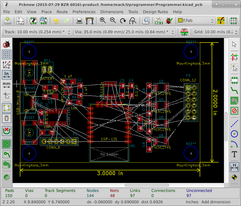
Once I finished with CvPCB, I loaded the PCB new program from the KiCad project manager. I clicked on the netlist button. I clicked on read current netlist and then close. The components were in a jumbled mess in the upper left corner of the layout sheet.
I selected all the footprints and drug them to the center of the sheet. Because I don’t have a form factor I am trying to fit, I am optimizing layout for minimal board space used. (this will cost the least)
I got the board down to 3″ x 1.5″ without any standoffs. I decided to size it up to 3″ x 2″ to make room for standoffs and modifications. I then rearranged for this new space. I tried to manage data flow from left to right across the board. I also tried to keep the antenna away from any components.