Preparing for fabrication and population Hardware V00F

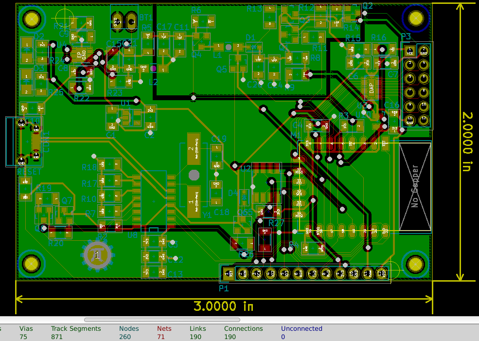
This week is about getting the files ready for ordering.  I thought about calling it Sometimes you have to do boring stuff II.  I’ve pushed an update to github so that fabrication files and the new BOM are available to download.

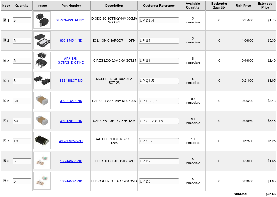
I started by running a BOM file from PCBnew.  I gave it a different name so that I could compare with the Last BOM. I opened the V00B file and then the new file called programmerV00F.  I set them up so I could see the differences.  There might be a good merge tool, but I don’t know of it.  Line by line I started going through the components.  Adding, removing, or updating each one. I deleted the lines that represented things that did not need to be ordered. This included the battery, mounting holes, and my logo. Once the obvious items had been taken care of, I went through it line by line and took counted my inventory of each item to make sure I had enough components to build one board.

I wrote the reference designator on each component bag as I went through the BOM.  This will save me time as I populate the PCB.  I found R5 in the BOM and I remembered I still need to experiment with it’s value, so I will pull it from a resistor kit. I skipped the charge indicator LEDs and their limiting resistors, I am not sure I want them yet. I changed my mind, I decided to get 5 each of the green and LEDs and I will use resistors out of my Resistor kit.
V00FDcartI ran the fabrication files to get gerber formatted layout files and the numerical drill file. I overwrote the older files because I knew that they were stored in a zip file. I then packaged them into a new zip file named UprogrammerV00F.zip.  I did a quick review of the output files, and I am ready to order.

I’d love to hear what your thoughts are on this design.

Parts Placement (Hardware V00E)

With the design review and testing done, it is time to update the layout.  I started by doing a Design rules check on the schematic. I got 3 errors, two were passives connected to inputs.  I changed the analog input of U10 Pin 3 to a passive pin. This is not a problem, but might be in other circuits. The third indicated two power outputs were connected together.  The CH340G has a 3 volt pin that operates as either a power input (3.3v operation), or as an output (5v Operation), I went in and edited it to be a bidirectional pin.  It still gave me a warning, but it’s acceptable.

Design rule warnings and errors are important, for each one, I will check to make sure it doesn’t represent a real problem and try to fix it.

I then ran CvPCB to confirm all devices have an assigned footprint.  I had made some changes that means a few new components, and footprints. I got all the parts assigned and saved them. then saved the schematic sheet. I then ran a netlist. I opened the layout design, and imported the new netlist… it gave me an error. It couldn’t find the library Housings_SOT-23_SOT-143_TSOT-6. The library name had changed, I went back into CvPCB and found the TO_SOT_Packages_SMD library that had the SOT23 footprint that I needed for all of my transistors. After making reassigning the footprints, I re-saved CvPCB and the schematic file, then generated a new netlist.

This left me with a bunch of parts all jumbled together. I started by spreading them out so I could see their ratsnest better. Once I saw how much components needed to be moved around, I ripped up all traces as well as the ground plane.  This gives me the freedom to re-arrange the board more efficiently.  My strategy was to start at each end of the board and work to the middle.

Looking at the design, the switch for upload takes up a lot of space and is not needed. I went back into the schematic and removed the upload switch. This required that I generate a new netlist and read it into PCBnew.

I left the USB connector where it was, put the Lithium cell in the NW corner, the Reset circuit in the SW corner, the wifi module in the SE corner, The test header along the south edge, the target connector on the NE corner and the high voltage circuit along the north edge.

PartsPlacementV00E

I routed the board using the interactive router. I then added my logo on to the board. I want to edit my logo a little bit, I may change that before I send the files off to fabrication.

FinishedLayoutV00E

The kicad files are on www.github.com, use the link just below my logo to download them.

Do you have any comments, would you do something differently,  can you see a better placement of parts?

Design testing for layout

I tested the battery charging circuit this week. It failed.  The lithium cell would charge, but when I disconnected the power adaptor everything shut down.  I didn’t understand how the enable lines worked.  In my hurry, I missed an example circuit in the datasheet that closely matched my needs. Most importantly it showed where to connect the enable lines for “normal” operation.

So for my client, I connected a diode from the out line of the chip to the in line of the chip(where the enables were connected to). The diode makes sure the out line is controlled by the chip and it can manage the current correctly.  Note D5 in the schematic below.

D5addition

This works but it is kind of a hack.  Hacks are great for testing prototypes, doing one off designs, and temporary changes.  Hacks lead to problems in production, if at all possible hacks should be avoided on production runs.  The right way to connect this circuit for both the programmer and my client is to connect EN and ENO to the +5V rail and ENBAT to the battery positive terminal.  This configuration means that anytime power is connected to the power, it will supply system voltage from the +5V supply and charge the lithium cell with whatever current is left from the 450 ma I limited it to.  When the +5V rail is not powered, or under powered,the lithium cell supplies current to system.

LithiumChargerFixed

I modified the code to connect the sigma delta to GPIO13 to drive the level shifter signal, then connected 5 Volts to the Vt and measured the waveform on the pad that corresponds with GPIO 13 through the level shifter. It didn’t work, Or the DSO138 oscilloscope can’t read the sigma delta signals.  I found a recommended power up sequence of the the level translator chip that I hadn’t considered before, the /OE pin should be brought low after power up.  This is to prevent excessive currents, I shouldn’t get the results I am seeing, I decided to try just toggling the GPIO12, 13, 14 pins controlled by the serial communications.  The system has gotten very unstable, I decided to re-flash the user config and wifi calibration data.  Turned out that Vt was/is shorted to ground, My best guess is the Pad directly under the chip solder bridged to the Vt(Vccb) pin of the level shifter chip.  Time to lay out again.

Do you have any Ideas or suggestions that might be useful for this design? Would you do anything differently?

Electronics design review (Hardware V00D)

The circuit is almost ready to go to layout again. This week I took a close look at the schematic design to look for errors and unfinished tasks.  By the way, you can put notes on a schematic to help you find anything you put off for later.

I have received the PCBs for my client, but I haven’t had the chance to populate the first one yet.  This means I haven’t had a chance to test the charging circuit yet. The availability of inexpensive PCB fabrication like OSH park has made a mini PCB test run reasonably priced.  You can now design a development board that exactly meets your requirements very inexpensively.  Since each iteration of the this design isn’t costing a lot, I am testing multiple changes each time. This allows me to work with devices that I am completely inexperienced at very low risk.

I started with the lithium cell charging circuit. I verified the input from the micro USB connector is tied to the input of the management chip.  I copied the timing and current limit device values from my client’s design.  The lithium cell (connector) is connected to GND and the dedicated pin on the management chip.  The status outputs are tied to LEDs so I have some indication of what is happening during charging. I may try to incorporate these signals later in the design. The system power output is connected to the 3.3V regulator which is working well on the two test boards I have already built.

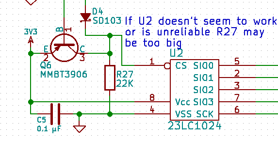
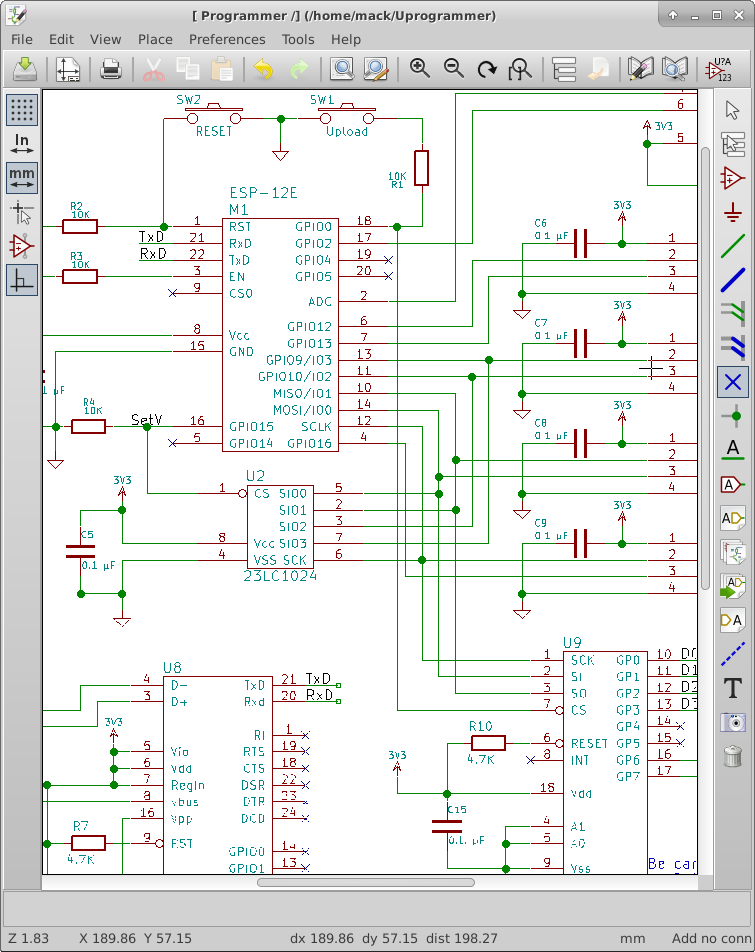
Next I looked at the SPI RAM Chip select logic.  The transistor Q6 turns on when CS0 is low; this pulls the chip select line for U2 high preventing U2 from contending with the SPI bus when the flash chip is being accessed.  There is a diode blocking the high from pulling GPIO15 high during reset. There is a pull down resistor for when GPIO15 is low and CS0 is high to activate U2 chip select. This is untested but the design looks like it will work.  I chose 22K resistors for the pulldowns on GPIO15 and U2 chip select as a balance between current required when GPIO15 is high and the speed at which U2 chip select will fall when released.  Since I don’t know the amount of capacitance of that circuit, I may have to change that resistor value later.  Good place to put a note on the schematic.

U2 Schematic notes

The level shifter U3 is untested, I should test it before I go to layout. Another note.

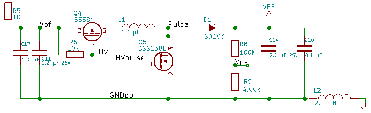
I decided earlier that the voltage booster was working but needs to have an isolated ground on the PCB layout.  I have added an inductor between the boost GND and the system GND.  This allows for some experimentation.  I can just bridge the pads with solder, I can put a resistor in there, or I can install the inductor. If isolating the GND is enough, that’s great.  The resistor would help provide better filtering but could cause problems.  The inductor is best filtering but will slow down signal transitions of the high voltage. I also gave the net name GNDpp to the isolated GND.

Vpp GNDpp isolation

The transistor driver for VPP is untested, because I haven’t had the positive voltage available. I could have attached a 12 volt source and tested it but it’s a simple circuit. It should work. The analog switch is working, nothing to review with it.

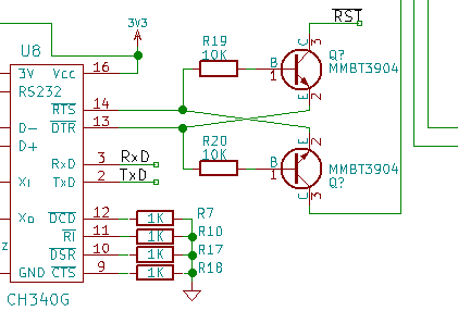
Finally, the programming control pins RST and GPIO0. I am not happy with the resistor connections. I have decided to copy the design from the NodeMCU dev board.  It is simple and works well on the dev board.  The only thing I am concerned about here is how much current the UART bridge pulls when not connected to USB.

CH340 Crossslink

Use the GitHub link to get a current copy of this design. After testing, I will go to layout.

I would love to hear any questions or suggestions.  If you would do this differently, please comment.

Code Cleanup and Boost Circuit testing (Firmware V00E)

This week I was reading through the SDK documentation, and realized a better way of handling serial events.  I was setting a flag and using a software timer to handle those events once a second. I also found that there is a webserver example in the IOT example.  I think this server is much simpler than ESP Ginx.  I have decided to try to use this example to move forward in the design

I decided to set up an OS task that I can post to that will do things like display the serial menu.  I am already using a task for serial handling.  (I grabbed it from an example and modified it for my uses).

I started by changing the UART task to a more generic task. I changed uart_recvTask to taskHandler. Then I just call an os_event_post with the action I want taken.  This allows the system to decide when to start the action. Displaying the menu and other tasks will generally happen faster this way.

As soon as I tried to do anything with GPIO16, I got lots of reboots.  It seems that the problems I was having with the Voltage boost circuit may have actually been GPIO16 problems. I have moved the control pin from GPIO16 to GPIO13 for enabling the voltage boost circuit.  With GPIO13 connected to the base of Q4 to enable/disable the boost circuit, the firmware booted and worked reliably.  After that I changed the filter resistor back to 10 Ohms as I had originally specified. And… It didn’t boot.

I replaced the 10 Ohm resistor with a 100 Ohm Resistor.  Still wouldn’t boot. I found that if I could get Q4 turned off, then the system would boot and run reliably.  As soon as I turned Q4 back on, the system would reboot and hang. So I tried adding a 100 μF between +BATT and GND to try to filter any electrical noise. It didn’t work.

I connected a bench power supply set at 3.3V to the boost circuit input, and I got it to partially work. I got 8 volts out of it for a few seconds.  I reinserted the GPIO16 initialization functions and no problems when no power is connected to the boost circuit.

I added some code that allows me to increment or decrement the prescaler using + and – keys respectively. When I hit the – key when the prescaler was at 0 to get to 255, it would reboot. When I hit the + key to go from 99 to 100 it would reboot.  So for now the prescaler is limited to the range of 0 to 99.

I am encouraged by getting the voltage on VPP higher than any supply voltage on the board. It appears that I need to create a separate ground plane just for the boost circuit.  If I couple it to the main ground with a low value inductor, I might be able to eliminate the problems it has caused.  I have uploaded the new version of the code. It still has very little commenting, however, I think it is cleaner and easier to read.

Web Server firmware

I am waiting on the stuff I ordered last week.  The CH340G chips are probably going to take the longest at 3 to 4 weeks.

To start with I updated my virtual machine to keep it current, I downloaded V1.5.0 of the Espressif SDK, and updated the lubuntu inside of the virtual machine.

I spent this week trying to get the chip running as a web server.  On the ESP8266 forum I found about a project called esp-ginx.  It is a web server with a lot of features.  For me it looks like a lot more than I need.  This is good for this design, I can cut away or ignore the features that I won’t be using or needed.

I downloaded the zip from github.  I ran make from the wrong directory and it failed to compile.  Finally realizing I need to run make from the project directory I was able to get it to compile without any errors.  I then uploaded it to my board and it didn’t work.  I was continuously getting fatal exception (0) on the serial port at 74800 baud.  Thinking that my RAM chip might be causing problems, I decided to remove it and try again.  Still no success.

I then tried to load the code into the NodeMCU board that I also use for testing. I got the same results with it.  I re-loaded my code into my board and got it back to working.  After many tries I finally realized tried putting the app folder in my home directory without any of the SDK files and it compiled.  I loaded this to my board with the commands: make clean, make html, make, and make flash.  The virtual machine had crashed and I needed to reboot my whole system before this worked for me.

This has been very frustrating just to find out that I didn’t understand the way to set up my files.  After I got the web server up and running, I added an entry to my hosts file on my computer.  I made an entry that pointed to he ip address of the board and associated it with smart.relay.com.

SmartRelay

Re-Layout Update V00B

Now that the design review is complete, I am updating the PCB layout.

I started by going into CvPCB to check and fix any components. I feel that the pad sizes are too large with the Handsoldering footprints.  I changed all 1206 Handsoldering footprints to 1206 standard  footprints. The 1×12 connector hasn’t been assigned yet, I chose a 0.100″ pin header footprint which I will leave empty. The Socket Strip 1×12 fit my needs.

While doing some research, I found a chip to replace the level shifter chips I was using.  The FXMA108 chip by Fairchild Semi does all 8 bits with automatic direction changing.  It’s capable of up to 80 Mb/s.  It allows me to simplify my design and remove the shift register.  Each buffer automatically shifts direction based on how its pins are being driven.  I removed the four level shifter chips and replaced them with this one chip. I had to create the chip in my library.

While moving parts around the layout, PCBnew shut down unexpectedly and I lost about 2 hours worth of work. There are so many changes to this layout that I decided to remove all of the traces and start new.  Under the edit menu is Global Deletions, I selected tracks and hit OK.

I moved the microUSB connector to hang off of the edge of the PCB and changed the slotted holes to round with the longest dimension used for the diameter of the circle. I moved the component values outside of the board boundary which helped remove some clutter from the board.

I started laying out the traces around the level shifter first because that section is straight forward.  Ikepth the schematic open so i could make quick changes on the schematic to simplify the layout. With each change I madeon the schematic, I would generate a new netlist and then read it into PCBnew. I made many component placement adjustments while routing the traces. I finished by doing a fill of the ground plane on the bottum side of the board.  This made a couple of unconnected nets stand out so I fixed them.Re-Layout V00B


Updating Schematic V00B

In the last few posts, I found several problems with the design as well as found some ways to reduce Bill of Material costs.  I also want to make soldering of the parts easier for a hobbyist.

I had problems using the CH340G chip on my NodeMCU board.  I couldn’t find any references to this problem on the internet.  So I replaced U8 (the CP2104 USB to UART bridge) with the CH340G USB to UART bridge.  I inverted DTR and RTS  and connected them to GPIO0 and RST respectively.  Using transistors as the inverters means that when U8 is not powered, it won’t draw those two lines down.  This is looking forward to when the design is battery powered.

I used the NodeMCU schematic as reference during this part of the design since it is close to what I want to do with this part of the design.

I changed the reset push-button switch to pads on the board and left the upload push-button switch unchanged but don’t plan on installing it unless I run into problems programming the board.

I also want to make things smaller, U9 is a large part of the board.  A shift register can do the same thing and be less expensive. I found the 74HC595 to replace U9. I am still clocking data in using the SPI bus, and then latching it with a pulse from GPIO5.

For the High voltage, I removed the AAT1230 and replaced it with two logic level FETs. One to disable the circuit to drop current draw when in low power mode connected to GPIO14. The other the pulse stream that generates the current through the inductor connected to GPIO4.  This means all the pins on the module are used up again.

Kicad schematic and layout can now be found here. The pcb layout is not current to the schematic, I still need to do a design review before I start the layout.

UProgrammerSchV00B

External RAM

I found a big mistake.  The pinout I had used for the design has the SPI pinout wrong.  This means that the External RAM and the Port expander will not work until I fix this issue.  So, I found an online layout image that shows the flash chip as well as the pins.  I used esptool.py to request the flash ID.  The Flash ID manufacturer code is C8 and the device code is 4016.  Using Google, I found this to be the GD25Q32 made by GigaDevice.  This is a 4MByte spi/qspi flash chip.  I looked up the datasheet and found the following pinout.

1 CS#-------VDD   8
2  SO|     |Hold# 7
3 WP#|     |SCLK  6
4 VSS-------SI    5

CS#.....Active Low Chip Select
SO......Serial Data Output/ IO1 (Quad/Dual IO)
WP#.....Active Low Write Protect/IO2 (QuadIO)
SI......Serial Data Input/IO0 (Quad/DualIO)
SCLK....Serial Data Clock
Hold#...Active Low Hold/IO3 (QuadIO)
VDD/VSS.Power Connections

Looking at the ESP-12E Module layout, I found the following connections by tracing the tracks:

Flash CS# is connected to Pin 9 — No Change

Flash SO is connected to Pin 10 — No Change (MISO)

Flash IO2 is connected to Pin 11 — Requires a Change

Flash SI is connected to Pin 14 — Requires a Change (MOSI)

FLash SCLK is connected to Pin 12 — Requires a Change

Flash IO3 is connected to Pin 13 — Requires a Change

I also discovered that if I want to use the Built in SPI Chip selects, I need to use GPIO0(CS2) or GPIO15(HSPI_CS).  TxD is CS1 which is a conflict for testing so I can’t use CS1.  I found this in esp8266 datasheet.

To fix the pinout on the schematic, I went into the library editor and just changed the pin numbers. I left the pin order in place for the schematic.

For the Chip Selects, I connected the RAM CS# to GPIO15(HSPI_CS) and the port expander to GPIO0(CS2).

I have some other schematic changes to make, I am still considering changing to the CH340G USB serial bridge.  The problems that I have had have given me reason to consider not using it.  I may have a faulty chip, I will test with another one, and if the problem goes away, I will feel more confident changing to the less expensive chip.

I have added the SPI and SPI overlay library code to the project source. No functionality has changed, so I am not uploading the code to GitHub yet.

HSPIconnections

Check Plots

Check plots are printouts of the design so that they can be verified.

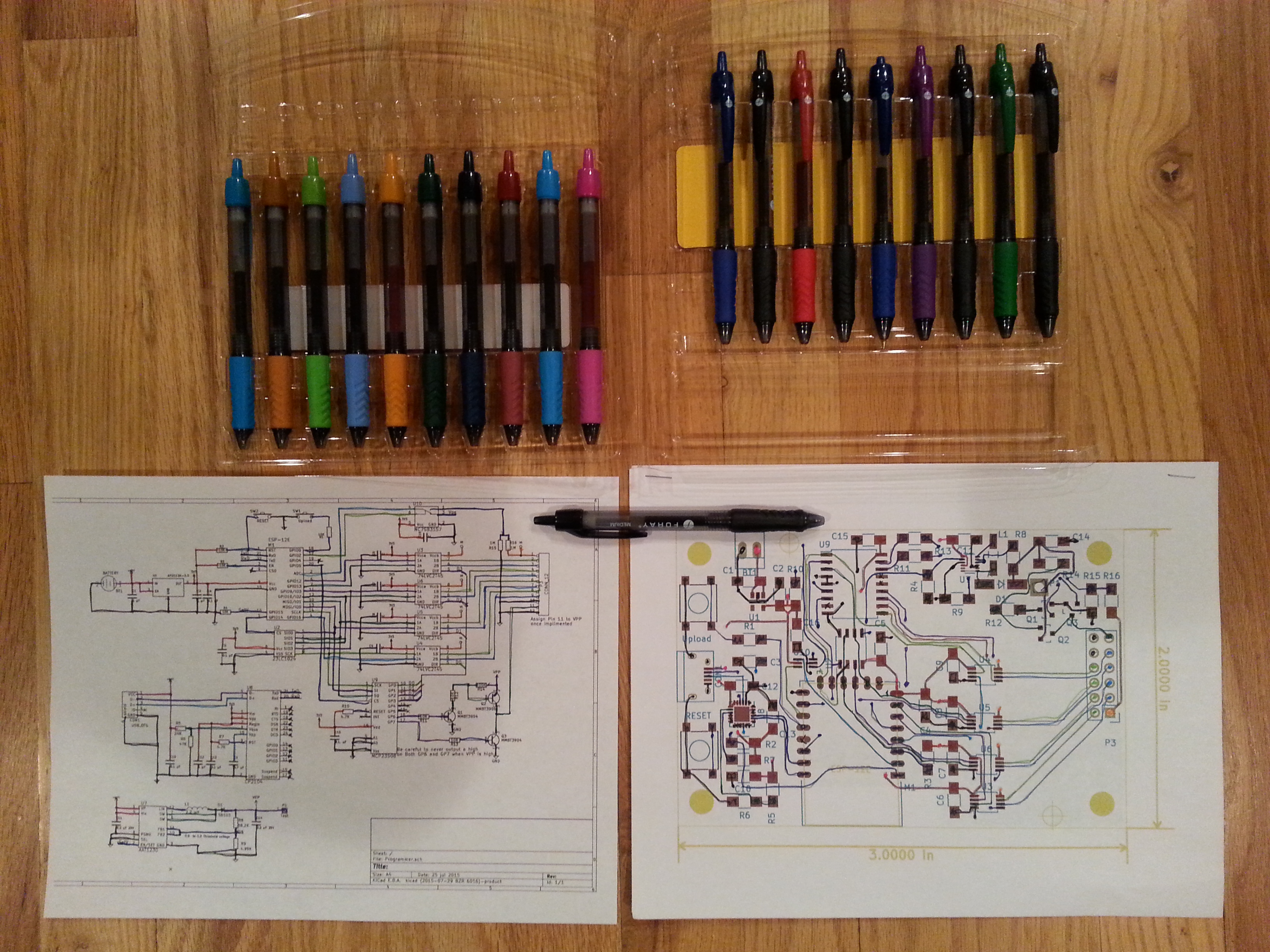
I printed out the schematic and both layers of the PCB layout as large as would fit on one letter sized page. Then I aligned and stapled the PCB layer plots together. I used colored pens to trace each circuit on the schematic and on the PCB layout.

In the first few minutes I found some problems. A bunch of references were not placed well, I found a section of the 3.3v net that did not get connected, and I had made a change that affected the ground plane fill that required me to redo the fill. I found these in the first half hour of verifying the check plots.  I continued to make adjustments as I checked the layout.

I printed a 1:1 scale to verify the ESP-12E would fit the pads correctly and it did fit. I generated the fabrication files by clicking on plot and clicked the plot button on that dialog, then I clicked on Generate drill file and made a drill file as well.  All these generated files were placed in a folder named “Fabrication” under the project directory.

Check Plots with Pens

1:1 Check Plot