Change in Design

I changed my mind, I think the programmer should be able to be reprogramed without any special tools.  This means that the Microchip processor is getting removed and replaced with a USB to serial bridge.  I have decided on the Silicon Labs CP2104 USB to serial bridge. My decision is based on cost and minimal external components. I went to several suppliers and compared 1K quantity prices.  I also confirmed that I can used the built in USB VID and PID.

I followed the example circuit in the datasheet for the CP2104 making minimal connections for a self powered device.  Since I am going to eventually have a battery that is the correct mode to wire for.

Since I no longer have the Microchip processor to control the high voltage, I connected the SET line of the AAT1230 to GPIO15 of the ESP12E.  The pulldown on GPIO15 will keep the voltage regulator disabled during a reset and I will drive it low anytime I am not using it, minimizing the current it draws from the battery.

I connected the Feedback voltage from the high voltage and the target voltage divider into an analog SPDT switch(NC7SB3157 chip) and connected the common terminal to the ADC input of the ESP-12E.  This allows me to verify what voltage the target system is at and what Vpp voltage is maintained during programming.  I ran out of IO pins on the ESP-12E, so I am added an SPI port expander(MCP23S08).  I have to give up 1 pin for chip select but I gain 8 general purpose IO pins.  So I moved the data direction control pins to the port expander and then connect GPIO5 to the CS line of the port expander. I verified the port expander could operate at 3.3V to match my operating voltage.

I connected GPIO2 to the Switch select line of the analog switch.  A high selects the VPP voltage divider, a low selects the Target voltage divider.  The voltage dividers are necessary because I could be dealing with more than the 3.3 V that the ESP-12E can handle.

None of the new devices were in the libraries.  I had to create each of the MCP23S08, the CP2104, and the NC7SB3157 in the schematic library.  I still have to connect the Vpp line to the target connector where I can leave it high impedance, set it to high Voltage, or Ground it.

USB Bridge and Vpp Port expander and Analog switch

Associating parts to pinouts

I ran the annotate schematic tool, then ERC to look for obvious mistakes.

I got a bunch of errors because I had left pins unconnected.  This is a reminder that I have to make sure these pins are set to outputs later.  I marked each unconnected pin with a no connect marker and I am down to 3 errors. I replaced the battery connector with a battery symbol.  It didn’t get rid of the error, I will have to check this connection on the netlist.

I then ran the netlist tool with default settings.

Then I ran the CvPCB module of KiCAD. I assigned footprints to the parts from the schematic.  Most of these matched.  For resistors and capacitors, I chose to use 1206 SMD for the footprints.  There is no footprint for the ESP-12E.

I found a footprint online for the module, but KiCAD would not import it. So, I created a footprint and added it to the custom library for the project.

I chose the SW_PUSH_SMALL for the two tactile switches Reset and Upload.  These are through hole footprints, I am thinking I will copy this footprint to the custom library and modify it to go surface mount.

I have only done very simple layouts.  This will be quite a learning experience for me.

CvPCB 1st

Multiplexing Pins

If you need just a few more pins on your design, one option is multiplexing.  Some chip manufacturers add multiplexing into their microcontrollers to add versatility.  Often however you have to choose between pin functions that you will use in your design.  For Instance the SPI Pins are shared with the I2C interface.  This can be hard to set up to use both.  If I have a target system that is programmed over I2C, I can use the buffers to isolate the I2c devices from the SPI bus when accessing memory.


I need to be able to pull GPIO0 low for reprogramming the ESP8266 module.  I have already assigned GPIO0 as an output to control the signal direction of the voltage buffers.  During boot it is an input to switch into boot loader mode.  I can pull it low to reprogram the module and let it float the rest of the time.  I have attached a resistor to GPIO0 and a switch to ground to pull it low when I want to reprogram the module. The resistor needs to be small enough to reliably pull the pin low during boot, but not small enough to cause damage when the pin is driving a high output.  As a rule of thumb a 10K resistor should work well.  I will have to experiment with it when I have an actual module to work with.

A 10K resistor will limit current drawn off the pin to 330µA. 3.3V / 10,000Ω = 330µA

I am almost out of pins and may have to do some more multiplexing.

I have ordered some ESP-12E modules and hope to be testing/playing with them soon.  I will probably temporarily stop working on the design and do a couple of Hello World projects.

A developer will make a simple project to test key steps of the design.  In programming this is usually an attempt to put the words “Hello World” somewhere he can see it.  This is called a “Hello World” project. For hardware, this can be as simple as flashing a LED. In this design flashing an LED would prove I could reprogram the device, and have a basic understanding of the build toolchain.

Initial Connections

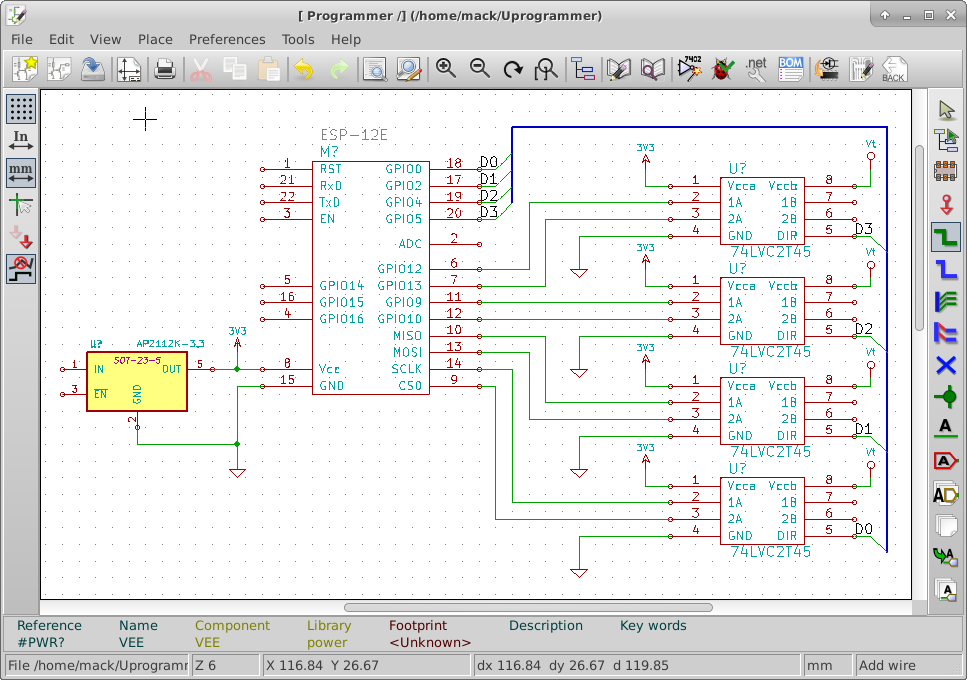
As I start connecting signals on the schematic, I look at which pins have dedicated functions.  The dedicated functions I need, I handle first.  This allows me to adjust the rest of the design around the required elements.  To make the schematic easier to read, I try to avoid crossing traces.


I went into the library editor and moved the pins of the ESP-12E around to make it easier to read the schematic.

I have connected the SPI pins from the ESP-12E to the level shifter chips.  I have also connected four GPIO pins to the level shifter chips.   I have placed the 3.3V power connections to each of the level shifter chips and the ESP-12E. I have also tied the 3.3V regulator to the 3.3V power bus. I connected GPIO0, GPIO2, GPIO4, GPIO5 to the direction pins of the level shifter chips.  I have also connected Vt to the level shifter chips. this voltage will come from the target to be programmed.

I have ordered 5 ESP-12E boards from Ebay.  I should receive them within 30 days.  Once I receive them, I will start doing a basic hello world project.

Initial Connections

Programming interface circuitry

The ESP-12E operates on a voltage between 3.0 and 3.5 Volts. The devices that I want this programmer to service could have operational voltages as low at 1.8 Volts and as high as 5 Volts.  Some routers operate on 12 Volts but their programming logic is probably in the 1.8 to 5.5 V range.


I searched for “level shifters” on the web and found a nice option from NXP.  The 74LVC2T45 is a dual supply, two bit Bi-directional buffer.  Maximum propagation delay is 10.1 nS  which would be compatible with JTAG speeds up to about 50 Mbps.  This would allow me to configure the I/O direction of each pair of bits at the connector.

Except for high voltage programming enable pins, These chips should be able to handle all the voltages for programming devices.  I will still have to design the programming enable voltage pins separately.

I am adding this new IC into the custom library and I will place several on the schematic.Interface Circuitry

TAPR Open Hardware License (OHL)

The TAPR Open Hardware License (OHL) is the only license I am considering that is written specifically for hardware and patent law.  It requires that any derivative works be licensed the same.  It requires distribution of all modified works to include the originals unmodified.


This license restricts what a developer can do with the design.  I am hoping that this product has enough value to developers that they would contribute to the design.  With that premise, I would not like other developers to be limited significantly on how they can use the intellectual property.

I am going to use the MIT license for both hardware and software.  I don’t need patent/copyright protection on this product.  Liability protection is a good thing, I intend this product to be “hackable”. Anything submitted to this blog for product design will be considered under the MIT license unless noted otherwise.

Experience and Heuristic method

Experience gives us a better chance at guessing solutions to a problem.

For instance a 220 Ohm resistor is a good rule of thumb for an LED current Limiting resistor in a 5 volt circuit.  A simple guess for a 10 volt circuit would be to just double the resistance to around 440 ohms.  Unfortunately this will probably burn out the LED.  From experience of doing the calculations, you would recognize that a 1000 ohm resistor usually works well in a 10 volt circuit.

Heuristic method comes in to play when you are working in an area that you are less experienced in.  You look at how similar operating circuits have worked in the past and make an educated guess to design the new circuit. Sometimes you just make a guess and then test, even with no reasoning as why that guess would work.

So if you are a tinkerer or an engineering student, go get some experience. Go build some circuits, make some changes, break something, then try to fix it or maybe improve it.