Re-Layout Update V00B

Now that the design review is complete, I am updating the PCB layout.

I started by going into CvPCB to check and fix any components. I feel that the pad sizes are too large with the Handsoldering footprints.  I changed all 1206 Handsoldering footprints to 1206 standard  footprints. The 1×12 connector hasn’t been assigned yet, I chose a 0.100″ pin header footprint which I will leave empty. The Socket Strip 1×12 fit my needs.

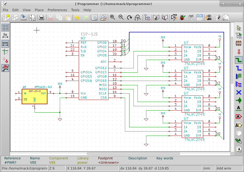
While doing some research, I found a chip to replace the level shifter chips I was using.  The FXMA108 chip by Fairchild Semi does all 8 bits with automatic direction changing.  It’s capable of up to 80 Mb/s.  It allows me to simplify my design and remove the shift register.  Each buffer automatically shifts direction based on how its pins are being driven.  I removed the four level shifter chips and replaced them with this one chip. I had to create the chip in my library.

While moving parts around the layout, PCBnew shut down unexpectedly and I lost about 2 hours worth of work. There are so many changes to this layout that I decided to remove all of the traces and start new.  Under the edit menu is Global Deletions, I selected tracks and hit OK.

I moved the microUSB connector to hang off of the edge of the PCB and changed the slotted holes to round with the longest dimension used for the diameter of the circle. I moved the component values outside of the board boundary which helped remove some clutter from the board.

I started laying out the traces around the level shifter first because that section is straight forward.  Ikepth the schematic open so i could make quick changes on the schematic to simplify the layout. With each change I madeon the schematic, I would generate a new netlist and then read it into PCBnew. I made many component placement adjustments while routing the traces. I finished by doing a fill of the ground plane on the bottum side of the board.  This made a couple of unconnected nets stand out so I fixed them.Re-Layout V00B


Multiplexing Pins

If you need just a few more pins on your design, one option is multiplexing.  Some chip manufacturers add multiplexing into their microcontrollers to add versatility.  Often however you have to choose between pin functions that you will use in your design.  For Instance the SPI Pins are shared with the I2C interface.  This can be hard to set up to use both.  If I have a target system that is programmed over I2C, I can use the buffers to isolate the I2c devices from the SPI bus when accessing memory.


I need to be able to pull GPIO0 low for reprogramming the ESP8266 module.  I have already assigned GPIO0 as an output to control the signal direction of the voltage buffers.  During boot it is an input to switch into boot loader mode.  I can pull it low to reprogram the module and let it float the rest of the time.  I have attached a resistor to GPIO0 and a switch to ground to pull it low when I want to reprogram the module. The resistor needs to be small enough to reliably pull the pin low during boot, but not small enough to cause damage when the pin is driving a high output.  As a rule of thumb a 10K resistor should work well.  I will have to experiment with it when I have an actual module to work with.

A 10K resistor will limit current drawn off the pin to 330µA. 3.3V / 10,000Ω = 330µA

I am almost out of pins and may have to do some more multiplexing.

I have ordered some ESP-12E modules and hope to be testing/playing with them soon.  I will probably temporarily stop working on the design and do a couple of Hello World projects.

A developer will make a simple project to test key steps of the design.  In programming this is usually an attempt to put the words “Hello World” somewhere he can see it.  This is called a “Hello World” project. For hardware, this can be as simple as flashing a LED. In this design flashing an LED would prove I could reprogram the device, and have a basic understanding of the build toolchain.

Initial Connections

As I start connecting signals on the schematic, I look at which pins have dedicated functions.  The dedicated functions I need, I handle first.  This allows me to adjust the rest of the design around the required elements.  To make the schematic easier to read, I try to avoid crossing traces.


I went into the library editor and moved the pins of the ESP-12E around to make it easier to read the schematic.

I have connected the SPI pins from the ESP-12E to the level shifter chips.  I have also connected four GPIO pins to the level shifter chips.   I have placed the 3.3V power connections to each of the level shifter chips and the ESP-12E. I have also tied the 3.3V regulator to the 3.3V power bus. I connected GPIO0, GPIO2, GPIO4, GPIO5 to the direction pins of the level shifter chips.  I have also connected Vt to the level shifter chips. this voltage will come from the target to be programmed.

I have ordered 5 ESP-12E boards from Ebay.  I should receive them within 30 days.  Once I receive them, I will start doing a basic hello world project.

Initial Connections

Programming interface circuitry

The ESP-12E operates on a voltage between 3.0 and 3.5 Volts. The devices that I want this programmer to service could have operational voltages as low at 1.8 Volts and as high as 5 Volts.  Some routers operate on 12 Volts but their programming logic is probably in the 1.8 to 5.5 V range.


I searched for “level shifters” on the web and found a nice option from NXP.  The 74LVC2T45 is a dual supply, two bit Bi-directional buffer.  Maximum propagation delay is 10.1 nS  which would be compatible with JTAG speeds up to about 50 Mbps.  This would allow me to configure the I/O direction of each pair of bits at the connector.

Except for high voltage programming enable pins, These chips should be able to handle all the voltages for programming devices.  I will still have to design the programming enable voltage pins separately.

I am adding this new IC into the custom library and I will place several on the schematic.Interface Circuitry