Understanding HSPI Firmware V00H

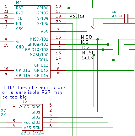
What I wasn’t understanding last week is the definition of HSPI_CS.  It is the same as CS0 in the HSPI module.  So when I turn on overlap mode, of course, it maps to SPI_CS0.  That leaves me with setting the HSPI to use CS1(GPIO1/U0TXD) or CS2(GPIO0).  Since I use U0TXD for reprogramming the module, CS1 is unavailable.

I cut the trace going to U2 CS0 and added a jumper wire to GPIO0.  I then changed the code to use CS2 to enable the RAM.  This included setting the HSPI to use CS2 and setting GPIO0 MUX to be SPICS2.  And I got what looks like a successful write to the SPI RAM.

Successful SPI Write

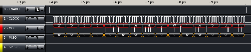
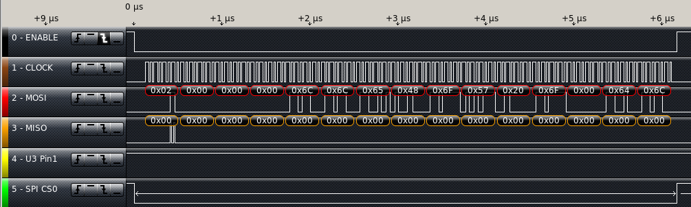
The byte command (2) followed by 24bit address (0) followed by the data.  The first four bytes of data are “lleH”.  This is backwards to what I was planning, I can change it by setting a bit or changing the bytes I put into the registers. As long as I read them back the same way, it really doesn’t matter as long as I read and write aligned to 4 byte words.  The data is one byte short, I had a typo sending only 11 bytes of data.

Note: When data is aligned to 4 bytes, it means you need to read or write only on increments of 4 bytes.  So you would only Write or Read to/from addresses that in hexadecimal end in 0, 4, 8, or C. Since this chip is a 32 bit processor, this is required often.

I then decided to implement the hard coded read command.  I copied the write code, changed the command from 2 to to 3, set the HSPI to read back  and zeroed out the working registers so that I can see if they have been filled with the data I stored in the RAM. Then I commented out the writeRam() call in user_init and added readRam() in it’s place. Doing this without powering down, I should get the data back without having to write it again. I forgot to switch the length to the receive length register; I fixed this then I got back all zeros for the data.

Unsuccessful SPI read

I see the command (3) followed by the address (0) followed by 12 Bytes of data(0). So I have more debugging to do.  My first guess is the WP or HOLD lines of the chip are not doing what I need them to do.

I have gotten a better understanding of the SPI hardware on the ESP8266.  It looks to me that I can get the same control by just using the main SPI channel to control my RAM chip.  This needs testing.  I will need to save any registers I change and restore them when I am done accessing the RAM.  This will also have to be done from code that runs from internal RAM.

I have put the current state of the code on GitHub.  Use the link under the search box on the right side of this page.

Have you used chips with similar SPI configuration?  I like that I can have any bit length of data on the SPI bus, this will be useful for JTAG data. Have you worked directly with JTAG data?

HSPI Frustrations

I cut the traces going to the SPI RAM that I figured out were wrong last week. On the PCB at U3 Pin3, and Pin5 I cut one trace each and on Pin6 I cut two traces.  Most of these cuts are under the chip so I made them before re-soldering the chip to the board.  Of course then I added wire jumpers to route the signals to match the schematic. I then added pins to connect the logic analyzer to.

Cut traces Chip Installed Rewired SPI


Last week I was looking at the the SPI driver code by MetalPhreak on Github as well as his blog to figure out how to send commands and data out and receive back over SPI.  The register SPI_USER is used to configure the SPI, SPI_USER1 sets up data length, SPI_USER2 sets up the command length and Command data.  Additionally, there is an SPI_Address Register that I can use to select an address in the RAM. Finally SPI_W0 to SPI_W15 are the data packet working registers — This is where I will put my “Hello World”.  I can write or read up to sixteen 4 byte words.  My RAM is organized in bytes so I will be putting bytes of data into the working registers.

So for initial setup I think the following should work for writing data.

SET_PERI_REG_MASK(SPI_USER(HSPI), SPI_CS_SETUP|SPI_CS_HOLD|SPI_USR_COMMAND|SPI_USR_ADDR|SPI_USR_MOSI);

CLEAR_PERI_REG_MASK(SPI_USER(HSPI), SPI_FLASH_MODE|SPI_USR_MISO);


The following should work for reading data:

SET_PERI_REG_MASK(SPI_USER(HSPI), SPI_CS_SETUP|SPI_CS_HOLD|SPI_USR_COMMAND|SPI_USR_ADDR|SPI_USR_MISO);

CLEAR_PERI_REG_MASK(SPI_USER(HSPI), SPI_FLASH_MODE|SPI_USR_MOSI);

The CS_SETUP and CS_HOLD parameters affect chip select timing. Setup is before clocking out data, hold is after.  Some chips need extra set up or hold time.  It will not affect performance significantly so I just turned each on by default so I don’t have to wonder if this RAM chip needs them. USR_COMMAND tells it to send the data in the command register. Likewise USR tells it to send the data in the Address Register.  USR_MOSI tells the hardware that there is data in the Working registers to be sent out. USR_MISO tells the hardware that I want to receive data into the working registers.

For the SPI RAM I want to send a command(Write), An Address(0), and 12 Bytes of data(“Hello World”).  This totals 16 bytes of data to be sent on the SPI bus:

1 byte for the command: 0x02
3 bytes for the address: 0x000000 and
12 bytes of data: “Hello World” including 1 trailing NULL.

For my first attempt to write to RAM I chose to hard code the instructions.
In my SPIRam.c File I had already created a function called writeRam.  I deleted it’s contents, and added the stuff to make this work.
void writeRam(char data[], int length){

SET_PERI_REG_MASK(SPI_USER(HSPI),
SPI_CS_SETUP|SPI_CS_HOLD|SPI_USR_COMMAND|SPI_USR_ADDR|SPI_USR_MOSI);
CLEAR_PERI_REG_MASK(SPI_USER(HSPI), SPI_FLASH_MODE|SPI_USR_MISO);

WRITE_PERI_REG(SPI_USER1(HSPI), (((12*8-1)&SPI_USR_MOSI_BITLEN)<<SPI_USR_MOSI_BITLEN_S)| //12 Bytes of data out
((7&SPI_USR_MISO_BITLEN)<<SPI_USR_MISO_BITLEN_S)| //Ignored for write
((23&SPI_USR_ADDR_BITLEN)<<SPI_USR_ADDR_BITLEN_S)); //address is 24 bits A0-A8

WRITE_PERI_REG(SPI_ADDR(HSPI),(uint32) 0x000000<<(32-24)); //write 24-bit address

WRITE_PERI_REG(SPI_USER2(HSPI),
(((7&SPI_USR_COMMAND_BITLEN)<<SPI_USR_COMMAND_BITLEN_S) | 0x02)); // Write Command

WRITE_PERI_REG(SPI_W0(HSPI),0x48656C6C); //"Hell"
WRITE_PERI_REG(SPI_W1(HSPI),0x6F20576F); //"o Wo"
WRITE_PERI_REG(SPI_W2(HSPI),0x6C6400); //"rld",NULL,NULL

SET_PERI_REG_MASK(SPI_CMD(HSPI), SPI_USR);// Tell hardware to do it.

}
After fixing my typos, I compiled and loaded the code.  The system booted without hanging. then I hooked up the logic analyzer to look for the data being transferred and it didn’t work. The Chip select line(U3 Pin1 ) doesn’t go low for a frame of data.  This means the chip never gets selected to write to.

With several hours of tinkering, I finally have it close, but it is still not working correctly.  The CS0 pin is being activated when the HSPI CS pin is being activated.  So I am getting the correct sequence of bytes when HSPI CS is low, but CS0 is low at the same time.

HSPI almost working

I have not posted a new copy of the software, I don’t believe it is useful to anyone yet.  It isn’t even useful to learn from.

Have you had similar frustrations? Have you gotten the HSPI to work in overlap mode?

Please leave a comment below.


ESP-12E pinout differences

A while ago, I found an e-book about the 8266.  It’s called “Kolban’s book on ESP8266” by Neil Kolban.  He compiled a lot of information on the ESP8266.  I decided to look at this book to see if it has any useful information concerning the HSPI.  It has very little to say about HSPI.  The book lists the API calls without any detail.  What is important is it lists a GitHub repository that has very easy to read example code.  The author of the example code also has a blog with a very good description of how to use the SPI registers.

Since I have the HSPI working with one byte, I decided to try to get the Overlap mode working before trying to add functionality.  I retested with the code from last week and got the same results. Let’s hear it for consistency!  Then I put the call to hspi_overlap_init() in my code just before the sending of data.  Without changing which pins the logic analyzer is attached to, I expect to see chip select to go low and but not see any clock or data, they should move to the other pins.  The data didn’t change pins.  I connected to the SPI bus to see if the data is being sent on both buses.  I checked what should be the clk line and got what looks like data. Next I checked what should be the MOSI line and it looks like the CLK line should look. I created the table below while doing the testing.  I did find that data was on both sets of pins.

Pin#(expected) — Most likely signal
PIN10(MISO) — ?
PIN11(IO2) — ?
PIN12(CLK) — ?
PIN13(IO3) — MOSI
PIN14(MOSI) — CLK

I grabbed the first build of the board to see if it acted the same. I soldered component leads to each of the SPI signals I was interested in and then attached the logic analyzer to those pins as I needed.  With the old board it looks like MOSI is on Pin13 and CLK is on Pin12.  There are definitely different pinouts of the ESP12E from (I assume) different manufacturers.  This could be a problem if I go to any kind of mass production.  There is a newer version of the chip ESP-12F that seems to match the pinout of the chip I currently have.  I don’t see any evidence on the web of different pinouts of the 12F yet.  This needs more research.

I will have to change the layout again but I can test the HSPI with RAM by cutting the traces and putting jumpers in to correctly wire the chip.  I went back and modified the schematics to reflect these changes.  Since the pinout for the 12F matches the lines I am pretty sure of, I used it to update the schematic.  I changed the labels on the Pins of the chip then changed the connections to the SPI RAM.

SPI Pinout FixESP-12F

Have you had to work with manufactures changing specs on you? Or obsoleting a chip? How did you deal with it?

Troubleshooting

I started out this week by hooking the SPI RAM to the logic analyzer. Then I hooked up the USB cable and it was stuck in a reboot cycle. I set the flash speed back to 20. Still stuck in reboot cycle. I disconnected the logic analyzer still in reboot loop.  I commented out the initSpiRam function in the startup code still stuck in reboot loop. This leads me to believe I have a power supply problem.

If it’s a power problem, adding large (100 μF) and small (0.01 μF) capacitors around the ESP-12E would solve the problem.  The 100 μF capacitor will act as an energy reservoir. The small capacitor will act as a noise filter. I piggy backed both a 100 μF and  a 0.01 μF capacitor on top of C4 the decoupling capacitor for the ESP-12E module. This didn’t solve the problem.  Next I suspected the SPI RAM was the problem.

I probed CS0 along with the SPI RAM CS line and they were in perfect phase.  This means that Q6 is not inverting the signal. This results with U2 on the SPI bus while the flash is being accessed.  That would definitely get it stuck in a reboot loop.  After feeling stumped for a while, I replaced Q6. It booted normally again. I uncommented the initSpiRam function and it started rebooting again. I tried with and without initSpiRam being called and it would consistently reboot when initSpiRam was called.

With initSpiRam uncommented, I went into the function and started commenting out lines to see what was causing the reboot.  It appears that ENABLE_SPI_DEV_CS() is causing the reboots. I moved it to after spi_master_init to see if that would work. spi_master_init(HSPI) by itself works. Next I tried adding overlap mode. It appears that overlap has to be after master init.  The SPI driver files and headers don’t have any way to read back data while in SPI master mode.

I decided to do a very simple test. I would do a SPI Master Write without overlap mode turned on. One write of one byte immediately after boot so it would be easy to catch on the logic analyzer.  The HSPI pins are:

GPIO14: CLK  Pin 5
GPIO12: MISO Pin 6
GPIO13: MOSI Pin 7
GPIO15: !CS  Pin 16

Chip select is the same pin I am already using, the rest are unconnected. I put a jumper across Q6 to always disable U2 by pulling CS (pin 1) high. I also soldered test points to each pin so I could easily attach the logic analyzer. With the jumper across Q6 I couldn’t even program the board!  This doesn’t make sense, I’ll have to come back to that.  I think I have some mis-wiring. I removed U2 from the board, and this allowed me to reprogram the PCB.

It now boots but doesn’t give me a menu. It appears to hang on the spi_mast_byte_write() call.

This is not a big deal, I haven’t set the SPI port.

All that time spent fighting this problem, and it turned out to be a solder bridge between R27 and a PCB trace from FLASH CS0.  I cleaned up this bridge and it started working reliably.

Finally I tested the basic HSPI write function. It didn’t work. but code is running without freezing or rebooting.  So I added a call to spi_master_init() still not working, no data on lines.  Looking in spi.c, I saw that spi_master_init() doesn’t assign pins to the HSPI port.  I added the lines below to user_init(). HSPI_PIN is defined as 2.

PIN_FUNC_SELECT(PERIPHS_IO_MUX_MTMS_U,HSPI_PIN); // GPIO14
PIN_FUNC_SELECT(PERIPHS_IO_MUX_MTDI_U,HSPI_PIN); // GPIO12
PIN_FUNC_SELECT(PERIPHS_IO_MUX_MTCK_U,HSPI_PIN);// GPIO13
PIN_FUNC_SELECT(PERIPHS_IO_MUX_MTDO_U,HSPI_PIN);// GPIO15

And I saw a byte on the logic analyzer. Yeah! progress.

SPI Byte outThe data speed is at 20MHz. I tried two writes in a row and got a chip select active for each write, and inactive in between. I need to figure out how to change this behavior, the SPI RAM commands always follow the falling(going active) edge of chip select. To write data to the RAM, I have to send more than one byte while chip select is active.

How do you do troubleshooting? Have you gotten HSPI Working on the ESP-12E? Does anyone know if there are different pinouts for the ESP-12E? Something I saw suggested to me that I still have the SPI RAM connected wrong again.

New PCBs

The PCBs arrived this week.  I really like the way my Logo came out.  20160415BarePCB

I do want to make an adjustment, make the arrows larger, they didn’t even show up on the silkscreen.

PCBLogo

To start testing, I put a jumper in bypassing the lithium cell charger. I then installed the ESP-12E, the SPI RAM, The Crystal, the USB Serial Bridge, the voltage regulator, and the USB connector. Just enough to power up, load a program and test the basics.

20160415assembledPCB

First test was to  connect to PC and run ESPlorer– it worked.

I got a message:


AT-based firmware detected.
AT+GMR
AT version:0.40.0.0(Aug 8 2015 14:45:58)
SDK version:1.3.0
Ai-Thinker Technology Co.,Ltd.
Build:1.3.0.2 Sep 11 2015 11:48:04

I then tried to install my test version of the software and it wouldn’t install.  I went back to ESPlorer and started playing with the DTR and RTS to see what would happen. It turns out I got DTR and RTS backwards. So I cut the traces and added a couple of jumpers. This is the kind of mistake I was hoping to catch in the design review.

It programmed great with the wires swapped. My code crashed, back to a “Hello World” version.

Turns out the internal memory chip installed on the ESP-12E does not run at the settings I had specified with esptool.py.  I found this out by setting it to 20MHz DIO mode which started working. I then switched it to QIO mode to see what happened. QIO worked, next I tried running at 40 MHz. That worked.

../esptool/esptool.py --port /dev/ttyUSB0 --baud 230400 write_flash -ff 40m -fm qio -fs 32m 0x00000 ../bin/eagle.flash.bin 0x40000 ../bin/eagle.irom0text.bin

I enabled HSPI Overlap mode by adding spiRamInit() to the end user_init(). Ran without crashing. When I started building for use, I discovered no SPI Master Read available.  I saw something that looked correct for slave read, so I borrowed a line from it and did a write followed by that line– it built. I uploaded the code, and it ran, still no testing of the SPI Ram.

I added the function calls to write “Hello World” to the SPI RAM. and read back and put out to the console. and I got garbage back to the console.  Not a surprise. Debugging with a logic analyzer next week.

Have you written code for the ESP8266. Have you worked with SPI before? I would love to Hear from you.


Hardware SPI test software (Firmware V00G)

The PCBs haven’t arrived yet.  So, I worked on the test code for the SPI ram.

Using the datasheet, I started setting up for SPI overlap mode.  On the ESP8266 there are two hardware SPI modules.  In overlap mode, they share the same pins.  This means that if you use the second SPI module you can directly work with the flash memory by using CS0 for the chip select.  I don’t see a lot of use for that other than for performance.  If you choose a different chip select, like I am using GPIO15. You are just sharing the pins with the processor. You have to make sure your code will run in RAM while using the second SPI.  ESP8266 documentation calls the second SPI HSPI.

From Microchips 23LC1024 datasheet, the sequence to write to the SPI RAM in sequential mode is:

Set CS low, write out the value 2 MSB First followed by the 24bit address to start writing at(in 3 bytes), followed by the data to be written(as many bytes as wanted up to the size of the RAM) followed by setting CS high.

A Sequential read has the following steps:

Set CS low, Write out the value 3 MSB first followed by the 24 bit address, then read in as many bytes as wanted. Then set CS high.

Side Note: MSB means Most Significant Bit.  Some protocols transfer in the opposite order or LSB first.  It is important to know this when setting up any serial communication. Data is clocked out on the falling edge of SCK and latched on the rising edge of SCK.  The inactive state of SCK is low.

To help out Espressif provides a guide called:

ESP8266 SPI Overlap & Display Application Guid

This guide describes the SPI Overlap mode API as well as gives a reference implementation using an LCD.  Unfortunately this document is missing a lot of useful information.  There is a post on Espressif’s forum describing it and showing an example.

To get started I have created two new files SPIRam.c and SPIRam.h.  This will make the code easier to locate and modify. To begin with I just want to write some data, and read it back and send it out on the serial connection. Basically a Hello World on the SPI RAM

I created 3 functions:

initSpiRam(); // Set up SPI and Overlap Mode
disableSpiRam(); // Shut down Overlap Mode
writeRam(char data[], int length);
readRam(char data[], int length);

I got it to build but I am unable to test it.

I still have to add a couple of commands over the serial port to tell it to write and tell it to read. I pushed a copy up to Github

I’d like to hear about the projects you are working on.  Please leave a comment below.

SPI RAM

I am anticipating the new PCBs coming in soon, (I have a tracking number but it doesn’t show up with Hong Kong Post or USPS). In light of this, I decided to do a little research on the SPI RAM so that when it gets here, I can quickly write code to test the functionality of the design.  The SPI RAM I have chosen is a 23LC1024.  A common manufacturer of this chip is MicroChip, I downloaded their datasheet for this chip and started looking at the process to write to and read from the RAM.

Notes for writing to SPI RAM:

Maximum 20 Mhz Clock for all data transfers (might cause me to slow down the FLASH)

Write speed only limited by clock speed.

Write command(0x02) followed by 24bit address followed by data

Page Mode 32bytes before sending a new address

Sequential mode can fill the whole RAM

Write is terminated by CS going inactive(HIGH)

Notes for reading from RAM

Same maximum clock speed.

read only limited by clock speed.

Read command(0x03) followed by 24bit address start receiving/clocking data from RAM

Three modes of operation, Byte, Page, and Sequential.

Byte mode only allows reading/writing one byte before having to resend an address.

Page mode all data is accessed in pages of thirty two bytes. Not very useful for this project.

Sequential mode allows access to all of RAM as one big block that I can start accessing from any point. I need to set the mode register bits 7 and 6 to 01.

I am going to start in standard SPI mode, Make sure it is working then adjust the code to start taking advantage of the SQI interface.

Making, Hacking, and or Engineering.

I am waiting for PCBs to come in and hardware testing is next on my agenda for the design. So, I wanted to explore the differences of Making, Hacking, and Engineering.

Dictionary.com Definitions:

Making:

1. the act of a person or thing that makes:

The making of a violin requires great skill.

Hacking:

8. Informal. to make use of a tip, trick, or efficient method for doing or managing (something): to hack a classic recipe;

to hack your weekend with healthy habits.

Engineering:
1. the art or science of making practical application of the knowledge of pure sciences, as physics or chemistry, as in the construction of engines, bridges, buildings, mines, ships, and chemical plants.
I of course picked the definitions relevant to this blog. Making requires skill but doesn’t necessarily have to be clever.  Hacking as used in the term “life hack” are clever or unusual ways of doing something efficiently.  Then finally Engineering is applying known science to a given goal. As an electronics designer, you are usually working in a blend of all three ways.
A few days ago, I did a little project that was basically all Making.  I wanted an inline set of controls for a wired headset that I already own. I looked up the requirements online, designed the schematic, and PCB layout and ordered PCBs.  I really didn’t do much engineering and it wasn’t particularly clever.
When designing something that has never been done before, Engineering is great, but sometimes falls flat. Perhaps the design hasn’t been done because no one has found a clever solution yet. An engineer has to be careful when they incorporate a hack into their design.  Often clever solutions have unforeseen drawbacks that may not become apparent until thousands of units have been produced.
Sometimes a design hasn’t been done because no one has seen the need for it before.  This is often a nearly pure engineering process. Nothing in the design is hard to do, but you have to know the science(or it’s shortcuts) to complete the design.
Side note: In some cultures Engineering is about individual and public safety. An Engineer’s job is to make sure a product or design won’t hurt someone. Although I think it is important to always be thinking about safety in your design, this is not part of this discussion.
Side Note: Scientific shortcuts speed up the design process.  For instance we know the left hand rule for figuring out the magnetic polarity of a coil given it’s direction of current flow.
Do you have any favorite science shortcuts? Are you a maker, a hacker, or an engineer?  Is there another way to look at creating something that you’d like to talk about?

Happy Pi day again

This is the second time this blog has passed by March 14th.  I am kind of a math geek, so it’s fun for me to celebrate.  And of course I chose PI as the symbol for this blog and my business.

I ordered PCBs and components this week. I selected Blue solder mask with white silkscreen from DF Robot, I chose 1.6mm board thickness, and ten boards. This costs US $26.95. The parts from digikey cost US $25.66 + shipping. keeping this iteration of the design’s material costs to under US $60 — not bad.

V00F DFRobot

I also registered my Business name (Prototype Iteration) with the state of Oregon this week.

I see that there are about 300 views of this blog each month. Are any of you in a similar stage of developing a project?  Are you ordering PCBs and components?  I look forward to hearing from you.

Preparing for fabrication and population Hardware V00F

This week is about getting the files ready for ordering.  I thought about calling it Sometimes you have to do boring stuff II.  I’ve pushed an update to github so that fabrication files and the new BOM are available to download.

I started by running a BOM file from PCBnew.  I gave it a different name so that I could compare with the Last BOM. I opened the V00B file and then the new file called programmerV00F.  I set them up so I could see the differences.  There might be a good merge tool, but I don’t know of it.  Line by line I started going through the components.  Adding, removing, or updating each one. I deleted the lines that represented things that did not need to be ordered. This included the battery, mounting holes, and my logo. Once the obvious items had been taken care of, I went through it line by line and took counted my inventory of each item to make sure I had enough components to build one board.

I wrote the reference designator on each component bag as I went through the BOM.  This will save me time as I populate the PCB.  I found R5 in the BOM and I remembered I still need to experiment with it’s value, so I will pull it from a resistor kit. I skipped the charge indicator LEDs and their limiting resistors, I am not sure I want them yet. I changed my mind, I decided to get 5 each of the green and LEDs and I will use resistors out of my Resistor kit.

V00FDcartI ran the fabrication files to get gerber formatted layout files and the numerical drill file. I overwrote the older files because I knew that they were stored in a zip file. I then packaged them into a new zip file named UprogrammerV00F.zip.  I did a quick review of the output files, and I am ready to order.

I’d love to hear what your thoughts are on this design.