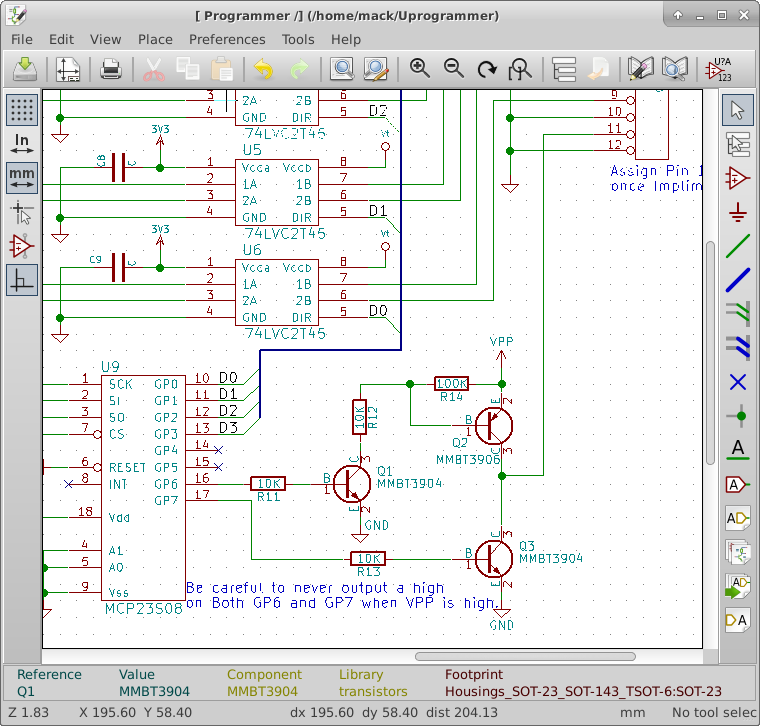
I am finishing up before going to layout. I implemented the high voltage design last week but wasn’t complete. I still need to control it going to the target. I looked at Microchip’s PicKit 3 as a reference design and pretty much copied the controlling transistors for my circuit design.
The drive of the high voltage to the target is turned on by a PNP transistor which is turned on by another NPN transistor. Grounding of the target Vpp is controlled by another NPN transistor. These transistors are controlled by GP6 and GP7 of the port expander.
It is important to note that things could get damaged if GP6 and GP7 were both turned on at the same time and the Boost voltage regulator is turned on as well.
I ran the annotation, then the electrical rules check, I got some errors. It found a bunch of unconnected pins that I hadn’t marked yet. I went back and marked them. I checked each remaining error and they are not really bad, but they needed to be checked anyhow. Then I ran the netlist tool. I then ran CvPCB to assign footprints to the new parts.
I hit the button to perform automatic footprint association, and I didn’t want to, It re-assigned footprints that I had already chosen. So I had to go back through the whole list verifying each component.
I finished by arranging the layout by watching the ratsnest as I placed the components in PCBnew. I am now considering this layout Version A, I have a lot of room for revisions.