Cost review

Newest SDK:

Espressif has moved the SDK to GitHub.  At this point, It is version 2.1.  I have no indication that they have done anything with the ADC Feature I requested.  I have not updated to this newest SDK yet. I will do that before I spend any time working on firmware.

New component costing:

The 74LVC2T45 level shifter chips are US $0.32 each in low quantities.  The PCA9306 I2C level shifter are about US $0.60 each in low quantities.  This results in the costs of the level shift components arount $1.50.  The original single part costs around US $1.25 each in low quantities.  This is not a big difference in cost but it does affect board space.

Design review:

Continue reading

Modifying the circuit for better Vpp control

Planning:

I needed finer control of Vpp.  Since this is an experimental design, I decided to make some calculated guesses to choose the right values.

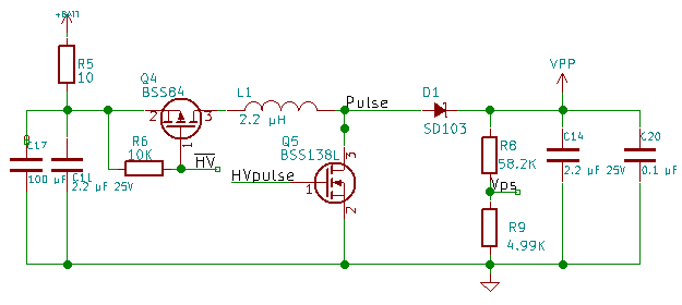
To start with, I believe that putting a resistor between the emitter and ground of the feedback transistor will limit the gain of the transistor.  The voltage of this resistor will rise as the current through it increases limiting the current gain of the circuit.  The first guess I tried was calculating the resistor as if the transistor wasn’t there(same as fully saturated) for my max voltage (25 V).

Continue reading

Cutting in the Vpp prototype

I opened my design schematic and realized I had already designed the Vpp control design. So now I have two options. I used an inductor in the first design to filter the base current of the voltage divider.  In the second design, I just used an RC low pass filter to filter the base current of the transistor.  This project has gone long enough that I am forgetting details of things I have already done.

Prototype Choice:

I prefer the design I did last week to the earlier design. If I find the system doesn’t regulate very well, I may incorporate parts of the earlier design.

Cut in Planning:

Looking at the last schematic and schematic where I want to end up, I can see I need to remove Q4, 5, R6 and R9. I then need to attach pin 1 of the FAN5331 to Pulse. Pin 2 to GND, Pin 3 to Vps. Pin 4 and 5 to the supply side of L1. Short Q4 Pin2 to 3. Finally replace R9 with a transistor with filter to HVPulse.

Continue reading

Lithium Charger Testing (Hardware V00I)

I installed the Lithium cell charger chip and it’s associated components.  While I was soldering the components, I noticed that R5 wasn’t soldered correctly.  This is the current limiting resistor for the voltage boost circuit.  So I need to retest the boost circuit.

I then attached the cell and the radio led blinked once.(with no connection, this was expected)  I connected the USB from my computer into the circuit and D2 (Red) lit up. This is STAT1 signal from the charger IC. From Table 5 in the AAT3672 datasheet STAT1 on by itself indicates the system is fast charging the lithium cell.  I disconnected the Cell with the USB still connected, both D3 and D2 blinked until I reconnected the lithium cell and the system then went back to fast charge.

I grabbed my DMM and checked some voltages:

From USB: 4.65V (A Little low, but I have connected the Uprogrammer to a long USB cable for convenience)
Output to Board: 4.65 V (Matches input voltage)
Lithium Cell: 3.96 V (Good range for Fast Charge)

These voltages make sense, I am very happy with these results.  I waited a while to check the results again.  While I was waiting, I started doing some testing of the Voltage Boost Circuit.  With Just the boost circuit turned on, I measured 4.64 Volts on Vpp.  I checked the Duty and prescaler and they were set to 0 and 4 respectively.

I then set the duty cycle  and measured the voltage at Vpp

20% : 19.6 Volts
30% : 20.8 Volts
40%: 21.8 Volts
50%: 22.6 Volts

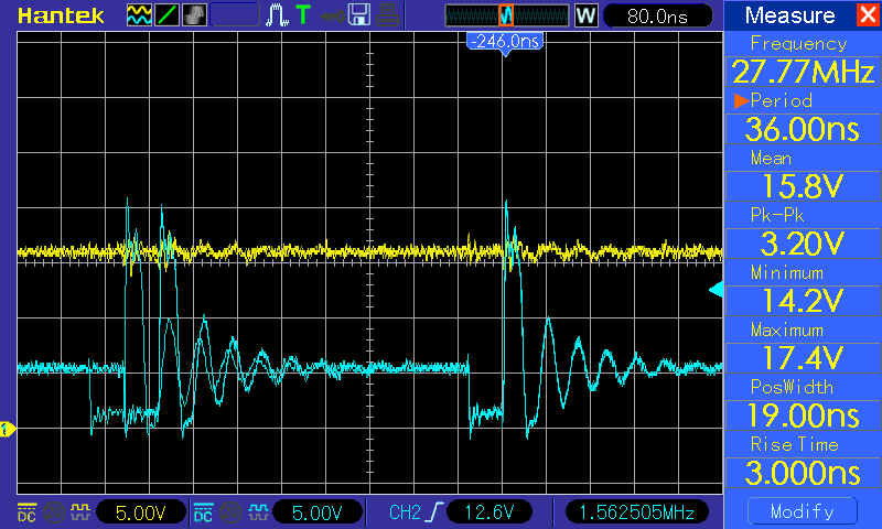
I played with the prescaler and the highest voltage I got was 24 Volts at 50% duty cycle and prescaler set to 9.  This is beyond design specification and has the potential to cause damage to the circuit, I don’t expect to do this in the future. I am happy to know that I have some margin in the design to if I need 20 Volts. I took the following image from my oscilloscope with a Prescaler of 4 and a duty cycle of 10% (25).

pre4duty25

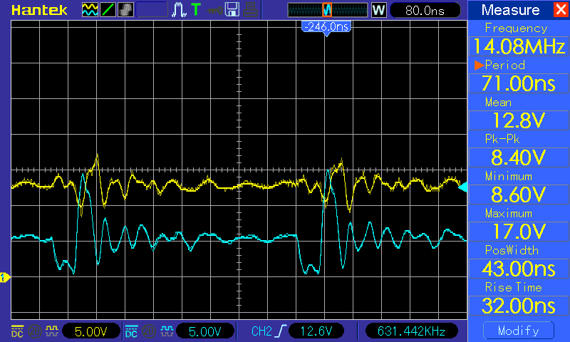
I am not happy with the large steps setting the output voltage of the boost circuit.  I decided to load the circuit with a 10 K Resistor to see how it affected the output voltage.  I soldered a 1206 10K Resistor on top of C20. This lowered the output voltage for 10% with a prescaler of 4 down to 12.8 Volts  But the best voltage I could get out of the system was 18 Volts.  This also made Vpp a lot noisier(See scope image below), I want to add some more filtering.

pre4duty25w10k

I added a resistor to the schematic parallel to C20 and also a place for another capacitor.  The resistor I set the value to 20K as a starting point and the capacitor I set to 1 uF.  The 20 K resistor will draw less current and that should reduce the noise.  The capacitor will also reduce the noise and provide a larger reservoir for current changes when programming a target device.

After doing all this testing the lithium cell voltage was at 4.12 V. This is near a complete charge, I expected the system to go to complete charge very soon. This is indicated by the Green LED being on alone.

After it switched to charge complete, I grabbed my DMM and checked some voltages:

From USB: 5.05V (Minimal current draw so no Voltage drop through the USB cable)
Output to Board: 5.05 V (Still matches input voltage)
Lithium Cell: 4.19 V (4.2 Volts is maximum charge voltage for individual LiPo Cells)

The charging circuit is working as expected.  I disconnected the USB and the LEDs turned off. I re-connected the USB and the Red LED came on for a few minutes and then it went back to only the green LED on.

I have uploaded the updated schematic to GitHub, click the hardware link in the right hand column to go get it.

Do you have a circuit you want to test before layout? Do you have a design you are tinkering with?

Hardware Iteration (hardware V00H)

The last time I worked on the electronics was when I got the switching boost circuit working.  The crashes I saw with it is why I did so much code work since then.  This week, I wanted to get back into electronics.  Since it has been a while I started by reviewing the schematic.  First thing I reviewed was the Lithium cell charger circuit.  It matches the reference design in the AAT3672 datasheet and it matches the PCB.  I should test it before I spin another set of boards.  I put a note on the schematic to remind myself to do that.

I then looked at the switched boost circuit. It turns out I don’t need L2, the real problem was in software. I removed L2 from the schematic. The resistor R5 was changed to 47 Ohms. I updated that on the schematic.  Next I looked at the USB to Serial Bridge, I have two cuts with Jumpers on the board, I checked them against the schematic. The schematic matches the patch I had made.

Next I compared the patches I made to the SPI RAM against a pinout of the ESP-12F I found online.  ESP-12F pins 9 – 14 on the schematic matches the PCB with the modifications I have made.  Pin 16 is no longer connected and Pin 18(GPIO0) is connected.  I had made this change back when I was testing the SPI RAM. With this change, D4, Q6, R26, and R27 are unnecessary. I removed them from the schematic and tied GPIO0 to U2 Pin1 and disconnected it from U10 Pin 6. I then tied GPIO15 to U10 Pin6 with a net label called A_SEL.  I have yet to test IO2 and IO3, Which will require running the RAM in QIO mode. In QIO mode, IO2/IO3 shouldn’t matter because when I read them back out of the RAM will come back out on the same pins they went in.

I have yet to test the level shift chip(U3).  I don’t like how hard U3 is to solder so I researched a different part to do the same thing. The new part I found is a TI TXB0108PWR which works very nearly the same as what I already had designed in but comes in a 20 pin TSSOP which is easier to solder.  The Pin order is different. The part is only US $1.88 in singles at Digikey.  I proceeded to change U3 to the new part on the schematic.  The datasheet recommends that OE be held low until both Vcca and Vccb are on.  I put a PNP transistor in to pull OE low anytime Vt is not driven.  As I dug into the datasheet, I found that this chip would not work for I2C.

So I did a little more research and I found another chip from TI.  The TXS0108EPWR works with SPI and I2C.  It has the same pinout as the TI TXB0108PWR so adding it to the schematic was really easy, I changed the name in the schematic.  This part is US $2.00 on Digikey.

txs0108esch

I uploaded the updated hardware design to Github. Click on the hardware link in the right column to go get it.

Have you used level shifters before? Have you decided on a chip only to find out that it was missing one crucial component? How did you fix it?

Code Documentation Firmware V00J

I Know that my code is very poorly documented.  So I want to focus on organizing and documenting the code.  To start with, I started looking for online classes that teach documenting code.

I found very little about commenting code.  I did find an interesting article I need to think about a bit more. The general theme of this article is to write code in such a way that comments should be rare.  For instance, code should probably be re-written if it needs comments to explain it. Variables should be named in a way that describes what they contain.

I was just about to give up searching. I was thinking I would start by putting header comments before each function or method.  This article gives pretty good reasoning not to do that. So this week, I decided to look at just one file — user_main.c.  Git does line by line version control.  I decided on one small header block at the beginning of the file.  This header block will indicate the license, original author, and/or the template source.

I looked to the header comments to know what to pass to and get back from a given function.  I have decided to make a new document that describes in better detail how to use each function.  This new file will be called UprogrammerFunctions.txt.  Since I removed the Comment block from in front of user_rf_cal_sector_set, That is the first function I am documenting in the API.

There is a big block of code in user_init() that all it does is set up the IOs to their initial states.  I copied that code into a new function called setup_io_pins() at the end of the user_main.c file. Next, I deleted all the test code I had commented out.  Finally, I made a couple of macros in user_config.h called VOLTAGE_BOOST_ENABLE()  and another one called VOLTAGE_BOOST_DISABLE()

Note: My definition of a macro is the use of a symbolic reference to represent other code.  In this place, I am using VOLTAGE_BOOST_ENABLE()  to represent  gpio16_output_set(0) to make it a little more clear what is going on. I also created a function in wifi.c to set up the wifi modem called wifi_init() and also put a prototype of wifi.init() in wifi.h.  I then moved the two wifi calls out of user_init() into the function wifi_init().

I tried to build and the call to the new function setup_io_pins() caused a linker error.  I needed to create a prototype of this function. I put it in user_config.h and it compiled, I uploaded it and it ran just like before I started cleaning up the code. I believe my user_main.c file is much more readable now.  I have uploaded the new version to GitHub. Click the firmware link in the right column of this page to go look at it or download it.

I would like to hear about your experiences cleaning up and commenting code.  What are your preferences for commenting code.

Firmware Stability with Voltage boost (Firmware V00H)

Since there seems to be some interplay between the SPI overlap mode and the Sigma Delta, I decided to disable the SPI RAM code to see if I can get the Voltage Boost working without crashes.  I used the // comment to make nullify the lines of code pertinent to the HSPI overlap mode.  Most IDEs let you select multiple lines and type CTRL-/ to comment out a block of code, and it toggles between commented and uncommented.

Note: IDE means Integrated Development Environment. Some IDEs are very advanced and checks if your code will compile while your are typing it in.  Others are just a simple editor with an integrated programmer/compiler.  In my case, I am using a program called Eclipse as my IDE.  It is very powerful as a code editor and I could automate compiling and uploading with it, but I have taken an easier path of making a few special shell files to automate the compiling/uploading process.

After commenting out the HSPI overlap code, I verified It would compile and run.  It compiled and ran. Good so far.  Next I started re-enabling the voltage boost circuit a little at a time. First, I turned of the FET allowing the current to flow into the boost circuit.  This is done by pulling GPIO16 low.  I did this by uncommenting two lines at the beginning of serial_init. (I also made a quick edit to a comment that was erroneous) I saved that and tried again. I measured Vpp at 2.75V.

The Sigma Delta Generator was set to a prescaler of 1 and duty of 0 from the last tests I had done.  Next I started changing the prescaler to see if the behavior has changed. 98 .. 99 .. 100 rst cause:2(Failure) Next I thought “maybe it’s the WiFi Modem”, So I disabled the modem.  I added the following three lines to the end of user_init()

    wifi_set_opmode(NULL_MODE);
    wifi_fpm_set_sleep_type (MODEM_SLEEP_T);
    wifi_fpm_open(); // force modem to sleep

98 .. 99.. 100 rst cause:2 (another failure)

Next I set GPIO16 to 1 in user_init() and commented it’s configuration out in seial_init(). Same result. Next I re-enabled system_set_os_print(). Maybe it’ll give me some useful message. No new messages came across the terminal emulator. I commented out the wifi_set_event_handler_cb() line. Still fails at 100.

So user_init() now:

sets the cpu frequency,
configures all the ports, including making sure all pins are disconnected from the sigma delta,
Initializes serial communications,
Initializes the Sigma Delta,
and disables the Modem.

cpu frequency is a system call,
Ports are just register writes,
serial communications are kinda of complex,
Sigma Delta is Just register writes,
and disabling the modem uses system calls.

This points to something in the serial communications.

Looking through the uart code, I noticed the ICACHE_FLASH_ATTR for uart_recvTask();  This is an ISR (interrupt service routine), and they shouldn’t reside in Flash, they should always be in ram.  I commented out the line and tried again. Again, same failure. I decided to sleep on it.

Moving forward, I continued to look at the serial communications code.  I decided to remove all the menu display code and just display the prescaler value with each keypress.  While making this change, I noticed that I had made a string buffer called outBuf of 32 bytes long. I used outBuf to format the Sigma Delta data before sending it out the serial port.  I counted it’s length, with a Duty of 0 and a Prescaler of 100 the terminating null character would be in position 35 of the buffer(That’s a buffer overrun).  I quickly shortened the string to leave the rest of the code intact and tried again.  And that solved it.

I re-enabled the menu.
Still working.

I re-enabled the boost voltage source.
Still working

Set the duty to  51(20%).
It is still working and I measured  2.72V at Vpp (2.72V doesn’t make sense)

Turns out I had both the Vpp drive and grounding transistors turned on causing the low voltage.  I set GPIO5 low and measured again with prescaler set to 4 and duty set to 102, I measured 22V on Vpp. Success!!!(little victory dance there)

I put a //TODO comment in my code to check everywhere I am using a string buffer for possibility of buffer overruns.

Putting a comment that starts with //TODO automatically adds it to a task list in the IDE. I can then go to the tasks list to see these notes. I now have stable but highly crippled code. I have uploaded the current state of the code to Github, click the firmware link in the right column to go get it or look at it.

When you are debugging do you have a technique that works especially well for you. Do you have a technique for finding buffer overruns? I would love to hear about your experiences.

Updating Schematic V00B

In the last few posts, I found several problems with the design as well as found some ways to reduce Bill of Material costs.  I also want to make soldering of the parts easier for a hobbyist.

I had problems using the CH340G chip on my NodeMCU board.  I couldn’t find any references to this problem on the internet.  So I replaced U8 (the CP2104 USB to UART bridge) with the CH340G USB to UART bridge.  I inverted DTR and RTS  and connected them to GPIO0 and RST respectively.  Using transistors as the inverters means that when U8 is not powered, it won’t draw those two lines down.  This is looking forward to when the design is battery powered.

I used the NodeMCU schematic as reference during this part of the design since it is close to what I want to do with this part of the design.

I changed the reset push-button switch to pads on the board and left the upload push-button switch unchanged but don’t plan on installing it unless I run into problems programming the board.

I also want to make things smaller, U9 is a large part of the board.  A shift register can do the same thing and be less expensive. I found the 74HC595 to replace U9. I am still clocking data in using the SPI bus, and then latching it with a pulse from GPIO5.

For the High voltage, I removed the AAT1230 and replaced it with two logic level FETs. One to disable the circuit to drop current draw when in low power mode connected to GPIO14. The other the pulse stream that generates the current through the inductor connected to GPIO4.  This means all the pins on the module are used up again.

Kicad schematic and layout can now be found here. The pcb layout is not current to the schematic, I still need to do a design review before I start the layout.

UProgrammerSchV00B