
I decided to try to use the SPI module instead of overlap mode this week. I went into the code that writes and reads from the SPI and changed the working registers to SPI in place of HSPI. I had to store and restore 6 variables in the writeRam() and readRam() functions. It worked but sent more data than expected. I noticed that I left the overlap init code in place, I removed it and tried again. I still got more data than I expected. I searched for HSPI and found one place that I had forgot to change it to SPI. I fixed that and now it is working. The code is also working without crashing.
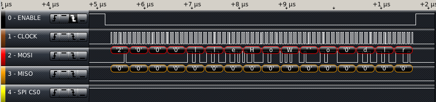
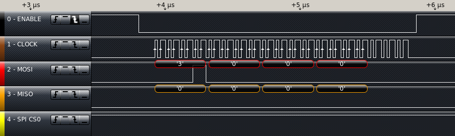
Next I added the read function back into the main code to see what would happen. I saw only 4 bytes on the SPI bus. I had missed a value change I needed to make the SPI read 12 bytes. It seems that either the DMA or an Interrupt routine is taking control of the SPI Hardware before i can finish a read. I disabled interrupts and it’s still only sending the command (3) and the address (0) plus 6 more clock cycles.
Since SPI is used for loading code into internal RAM as well as running it directly from flash, it might be difficult to figure out when I can use it for the SPI RAM. I had the HSPI appearing to work in overlap mode. Since I can switch between overlap and normal mode on the fly, maybe the HSPI in overlap mode is the best choice. In the writeRam() and readRam() functions, I changed the all references to SPI Registers to HSPI Registers and I commented out the code to save and restore the SPI Registers. I used find and replace to simplify the changes. I searched on (SPI) and filled in the replace with (HSPI) and then I selectively hit REPLACE/FIND for each instance.
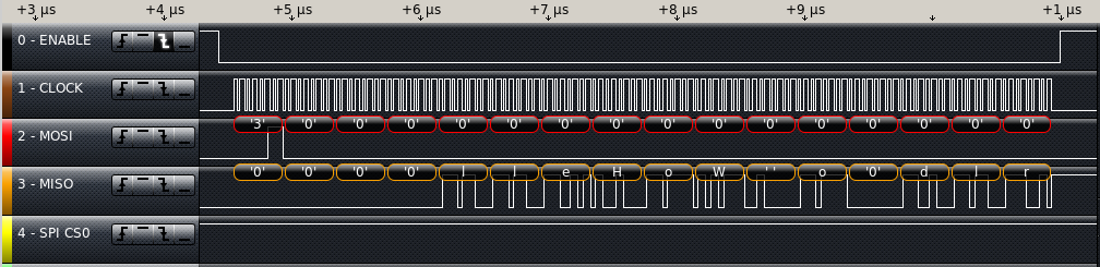
Then I built and tested the code, hopefully back to where I was last week. I got all zeros but I hadn’t done a write since I started working on it this time. So I put the writeRam() just before the readRam() in user_init() and tried again. On the logic analyzer, the write looks exactly like I would expect. The read is still not getting anything but zeros for the data section. Next step is to look at the HOLD and WP lines on the SPI RAM. I had to look at the datasheet to see what state they needed to be in to work correctly. Looking at the datasheet, there is no WP line, but there is a HOLD line. If HOLD is low, the serial interface of the chip doesn’t work. I clipped one more logic analyzer line on to Pin 7 of the SPI RAM. The signal looks identical to MOSI. I should have cut the trace when I was re-wiring this board but I missed it. I proceeded to cut it and add a jumper from the HOLD line to the ESP12E Pin 11. this is my best guess for the pins to use SQI. With Re-testing I got a successful read from the chip.
Next week, I need to verify the SPI working registers have the expected values from the ram. I put the current version of the code up on GitHub.
How do you handle cutting in circuit changes? Do you have any stories about a design change only to find it best to go back to the original plan?